SBOS740A May 2017 – May 2019 TMP116
PRODUCTION DATA.
- 1 Features
- 2 Applications
- 3 Description
- 4 Revision History
- 5 Pin Configuration and Functions
- 6 Specifications
-
7 Detailed Description
- 7.1 Overview
- 7.2 Functional Block Diagrams
- 7.3 Feature Description
- 7.4 Device Functional Modes
- 7.5
Programming
- 7.5.1 EEPROM Programming
- 7.5.2 Pointer Register
- 7.5.3 I2C and SMBus Interface
- 7.6
Registers Map
- 7.6.1
Register Descriptions
- 7.6.1.1 Temperature Register (address = 00h) [default reset = 8000h]
- 7.6.1.2 Configuration Register (address = 01h) [Factory default reset = 0220h]
- 7.6.1.3 High Limit Register (address = 02h) [Factory default reset = 6000h]
- 7.6.1.4 Low Limit Register (address = 03h) [Factory default reset = 8000h]
- 7.6.1.5 EEPROM Unlock Register (address = 04h) [reset = 0000h]
- 7.6.1.6 EEPROM1 Register (address = 05h) [reset = XXXXh]
- 7.6.1.7 EEPROM2 Register (address = 06h) [reset = XXXXh]
- 7.6.1.8 EEPROM3 Register (address = 07h) [reset = 0000h]
- 7.6.1.9 EEPROM4 Register (address = 08h) [reset = XXXXh]
- 7.6.1.10 Device ID Register (address = 0Fh) [reset = 1116h]
- 7.6.1
Register Descriptions
- 8 Application and Implementation
- 9 Power Supply Recommendations
- 10Layout
- 11Device and Documentation Support
- 12Mechanical, Packaging, and Orderable Information
Package Options
Refer to the PDF data sheet for device specific package drawings
Mechanical Data (Package|Pins)
- DRV|6
Thermal pad, mechanical data (Package|Pins)
Orderable Information
8.1.1.2.2 Self-Heating Effect (SHE)
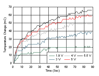
During ADC conversion some power is dissipated that heats the device despite the small power consumption of the TMP116. Consider the self-heating effect (SHE) for certain precise measurements. Figure 42 shows the device SHE in still air at 25°C after the supply is switched on. The device package, is soldered to the 11-mm × 20-mm × 1.1-mm size coupon board. The board is located horizontally, with the device on top. The TMP116 is in continuous conversion mode with 64 sampling averaging and zero conversion cycle time. There is no digital bus activity aside from reading temperature data one time each second. As shown in Figure 42, the SHE stabilization time in still air is greater when the device dissipates more power.

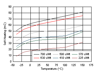
The SHE drift is strongly proportional to the device dissipated power. The SHE drift is also proportional to the device temperature because the consumption current with the same supply voltage increases with temperature. Figure 43 shows the SHE drifts versus temperature and dissipated power at 25°C for the same coupon board and the same conditions described previously.

To estimate the SHE for similar size boards, calculate the device consumption power for 25°C and use the corresponding power line shown in Figure 43. For example, in CC mode without duty cycle at a 3.3-V supply at 25°C, the device dissipates 410 µWt. So self-heating in still air is approximately 40 m°C for the described condition and rises to 52 m°C at 150°C.
The following methods can reduce the SHE:
- System calibration removes not only the self-heating error and power-supply rejection ratio (PSRR) effect but also compensates the temperature shift caused by the thermal resistance between the device and the measured object.
- If practical, use the device one-shot mode. If continuous conversion is needed, use the conversion cycle mode with significant standby time. For example, in most cases an 8-sample averaging (125 ms) with a 1-second conversion cycle provides enough time for the device to cool down to the environment temperature and removes the SHE.
- Use the minimal acceptable power supply voltage.
- Use a printed-circuit board (PCB) layout that provides minimal thermal resistance to the device.
- Avoid using small-value pullup resistors on the SDA and ALERT pins. Instead, use pullup resistors larger than 2 kΩ.
- Ensure that the SCL and SDA signal levels remain below 10% or above 90% of the device supply voltage.
- Avoid heavy bypass traffic on the data line. Communication to other devices on the same data line increases the supply current even if the device is in SD mode.
- Use the highest available communication speed.