SNOSD82D June 2018 – September 2022 TMP117
PRODUCTION DATA
- 1 Features
- 2 Applications
- 3 Description
- 4 Revision History
- 5 Pin Configuration and Functions
- 6 Specifications
-
7 Detailed Description
- 7.1 Overview
- 7.2 Functional Block Diagrams
- 7.3 Feature Description
- 7.4 Device Functional Modes
- 7.5
Programming
- 7.5.1 EEPROM Programming
- 7.5.2 Pointer Register
- 7.5.3 I2C and SMBus Interface
- 7.6 Register Map
- 8 Application and Implementation
- 9 Power Supply Recommendations
- 10Layout
- 11Device and Documentation Support
- 12Mechanical, Packaging, and Orderable Information
Package Options
Refer to the PDF data sheet for device specific package drawings
Mechanical Data (Package|Pins)
- DRV|6
- YBG|6
Thermal pad, mechanical data (Package|Pins)
Orderable Information
7.5.3.1.8 Timing Diagrams
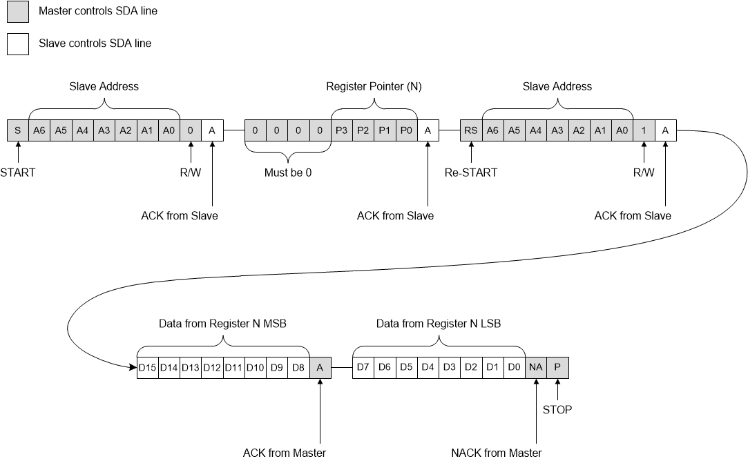
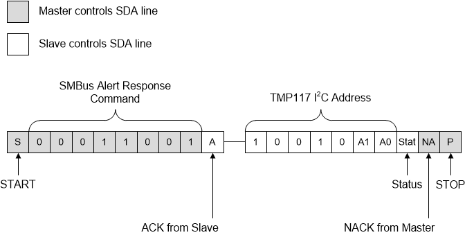
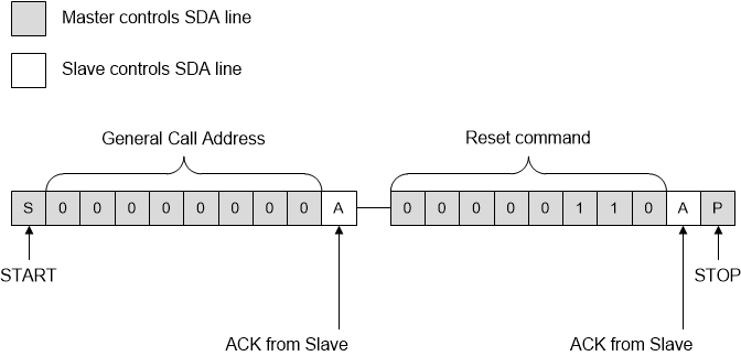
The TMP117 is two-wire, SMBus and I2C interface-compatible. Figure 7-9 to Figure 7-12 show the various operations with the TMP117. Bus definitions are:
Bus Idle: Both SDA and SCL lines remain high.
Start Data Transfer: A change in the state of the SDA line from high to low when the SCL line is high defines a START condition. Each data transfer is initiated with a START condition.
Stop Data Transfer: A change in the state of the SDA line from low to high when the SCL line is high defines a STOP condition. Each data transfer is terminated with a repeated START or STOP condition.
Data Transfer: The number of data bytes transferred between a START and a STOP condition is not limited and is determined by the master device.
Acknowledge: Each receiving device, when addressed, is obliged to generate an acknowledge bit. A device that acknowledges must pull down the SDA line during the acknowledge clock pulse in such a way that the SDA line is stable low during the high period of the acknowledge clock pulse. The user must take setup and hold times into account. On a master receive, the termination of the data transfer can be signaled by the master generating a not-acknowledge (1) on the last byte transmitted by the slave.
 Figure 7-9 Write Word Command Timing Diagram
 Figure 7-10 Read Word Command Timing Diagram
 Figure 7-11 SMBus ALERT Timing Diagram
 Figure 7-12 General-Call Reset Command Timing Diagram