SNOSD82D June 2018 – September 2022 TMP117
PRODUCTION DATA
- 1 Features
- 2 Applications
- 3 Description
- 4 Revision History
- 5 Pin Configuration and Functions
- 6 Specifications
-
7 Detailed Description
- 7.1 Overview
- 7.2 Functional Block Diagrams
- 7.3 Feature Description
- 7.4 Device Functional Modes
- 7.5
Programming
- 7.5.1 EEPROM Programming
- 7.5.2 Pointer Register
- 7.5.3 I2C and SMBus Interface
- 7.6 Register Map
- 8 Application and Implementation
- 9 Power Supply Recommendations
- 10Layout
- 11Device and Documentation Support
- 12Mechanical, Packaging, and Orderable Information
Package Options
Refer to the PDF data sheet for device specific package drawings
Mechanical Data (Package|Pins)
- DRV|6
- YBG|6
Thermal pad, mechanical data (Package|Pins)
Orderable Information
7.4.4.2 Therm Mode
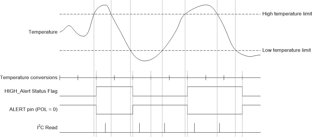
When the T/nA bit in the configuration register is set to 1 the device is in therm mode. In this mode, the device compares the conversion result at the end of every conversion with the values in the low limit register and high limit register and sets the HIGH_Alert status flag in the configuration register if the temperature exceeds the value in the high limit register. When set, the device clears the HIGH_Alert status flag if the conversion result goes below the value in the low limit register. Thus, the difference between the high and low limits effectively acts like a hysteresis. In this mode, the LOW_Alert status flag is disabled and always reads 0. Unlike the alert mode, I2C reads of the configuration register do not affect the status bits. The HIGH_Alert status flag is only set or cleared at the end of conversions based on the value of the temperature result compared to the high and low limits.
As in alert mode, configuring the device in therm mode also affects the behavior of the ALERT pin. In this mode, the device asserts the ALERT pin if the HIGH_Alert status flag is set and deasserts the ALERT pin when the HIGH_Alert status flag is cleared. In therm mode, the ALERT pin cannot be cleared by performing an I2C read of the configuration register or by performing an SMBus alert response command. As in alert mode, the polarity of the active state of the ALERT pin can be changed if the user adjusts the POL bit setting in the configuration register.
Thus, this mode effectively makes the device behave like a high-limit threshold detector. This mode can be used in applications where detecting if the temperature has gone above a desired threshold is necessary. Figure 7-6 shows a timing diagram of this mode.
 Figure 7-6 Therm Mode Timing Diagram