SNIS236 January 2024 TMP119
PRODUCTION DATA
- 1
- 1 Features
- 2 Applications
- 3 Description
- 4 Device Comparison
- 5 Pin Configuration and Functions
- 6 Specifications
-
7 Detailed Description
- 7.1 Overview
- 7.2 Functional Block Diagram
- 7.3 Feature Description
- 7.4 Device Functional Modes
- 7.5
Programming
- 7.5.1 EEPROM Programming
- 7.5.2 Pointer Register
- 7.5.3 I2C and SMBus Interface
- 8 Application and Implementation
- 9 Device and Documentation Support
- 10Revision History
- 11Mechanical, Packaging, and Orderable Information
Package Options
Refer to the PDF data sheet for device specific package drawings
Mechanical Data (Package|Pins)
- YBG|6
Thermal pad, mechanical data (Package|Pins)
Orderable Information
7.5.1.2 Programming the EEPROM
To prevent accidental programming, the EEPROM is locked by default. When locked, any I2C writes to the register map locations are performed only on the volatile registers and not on the EEPROM.
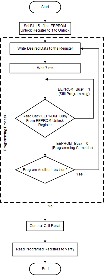
Figure 7-8 shows a flow chart describing the EEPROM programming sequence. To program the EEPROM, first unlock the EEPROM by setting the EUN bit in the EEPROM unlock register. After the EEPROM is unlocked, any subsequent I2C writes to the register map locations program a corresponding non-volatile memory location in the EEPROM. Programming a single location typically takes 7ms to complete and consumes 230µA. Do not perform any I2C writes until programming is complete. During programming, the EEPROM_busy flag is set. Read this flag to monitor if the programming is complete. After programming the desired data, issue a general-call reset command to trigger a software reset. The programmed data from the EEPROM are then loaded to the corresponding register map locations as part of the reset sequence. This command also clears the EUN bit and automatically locks the EEPROM to prevent any further accidental programming. Avoid using the device to perform temperature conversions when the EEPROM is unlocked.
 Figure 7-8 EEPROM Programming Sequence