SBOS335F June 2005 – January 2023 TMP300
PRODUCTION DATA
- 1Features
- 2Applications
- 3Description
- 4Revision History
- 5Pin Configuration and Functions
- 6Specifications
- 7Detailed Description
- 8Device and Documentation Support
- 9Mechanical, Packaging, and Orderable Information
Package Options
Mechanical Data (Package|Pins)
Thermal pad, mechanical data (Package|Pins)
- DCK|6
Orderable Information
7.2.3 Analog Temperature Output
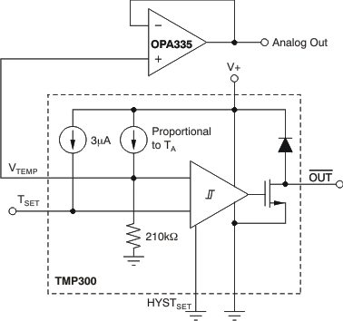
The analog out or VTEMP pin is high-impedance (210 kΩ). Avoid loading this pin to prevent degrading the analog out value or trip point. Buffer the output of this pin when used for direct thermal measurement. Figure 7-2 shows buffering of the analog output signal.
 Figure 7-2 Buffering the Analog Output Signal