SBOS371B August 2006 – October 2014 TMP401
PRODUCTION DATA.
- 1 Features
- 2 Applications
- 3 Description
- 4 Revision History
- 5 Pin Configuration and Functions
- 6 Specifications
- 7 Detailed Description
- 8 Application and Implementation
- 9 Power-Supply Recommendations
- 10Layout
- 11Device and Documentation Support
- 12Mechanical, Packaging, and Orderable Information
Package Options
Mechanical Data (Package|Pins)
- DGK|8
Thermal pad, mechanical data (Package|Pins)
Orderable Information
7 Detailed Description
7.1 Overview
The TMP401 is a dual-channel digital temperature sensor that combines a local die temperature measurement channel and a remote junction temperature measurement channel in a single VSSOP-8 package. The TMP401 is two-wire- and SMBus interface-compatible and is specified over a temperature range of –40°C to +125°C. The TMP401 contains multiple registers for holding configuration information, temperature measurement results, temperature comparator limits, and status information.
User-programmed high and low temperature limits stored in the TMP401 can be used to monitor local and remote temperatures to trigger an over- and undertemperature alarm (ALERT). Additional thermal limits can be programmed into the TMP401 and used to trigger another flag (THERM) that can be used to initiate a system response to rising temperatures.
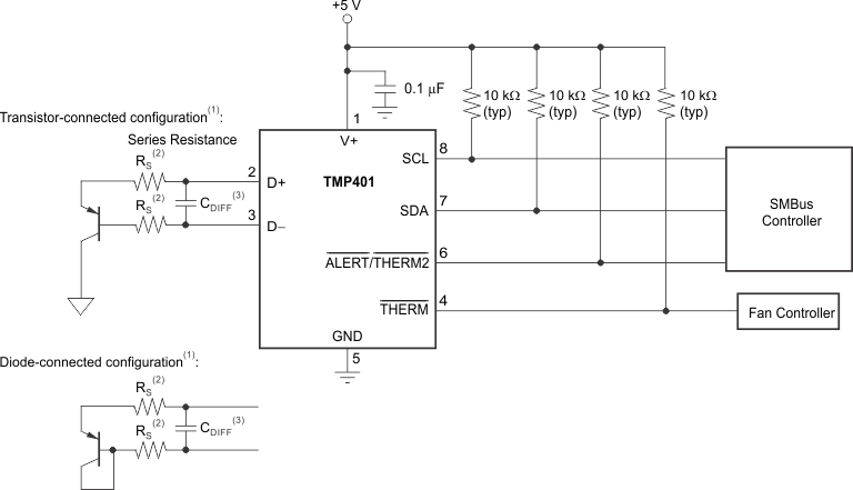
The TMP401 requires only a transistor connected between D+ and D– for proper remote temperature sensing operation. The SCL and SDA interface pins require pull-up resistors as part of the communication bus, while ALERT and THERM are open-drain outputs that also need pull-up resistors. ALERT and THERM may be shared with other devices if desired for a wired-OR implementation. A 0.1-μF power-supply bypass capacitor is recommended for good local bypassing. Figure 11 shows a typical configuration for the TMP401.
7.2 Functional Block Diagram
7.3 Feature Description
7.3.1 Standard and Extended Temperature Measurement Range
Temperature measurement data are taken over a default range of 0°C to +127°C for both local and remote locations. Measurements from –55°C to +150°C can be made both locally and remotely by reconfiguring the TMP401 for the extended temperature range. To change the TMP401 configuration from the standard to the extended temperature range, switch bit 2 (RANGE) of the configuration register from low to high.
Temperature data resulting from conversions within the default measurement range are represented in binary form, as shown in Table 1 (see the Standard Binary column). Note that any temperature below 0°C results in a data value of zero (00h). Likewise, temperatures above +127°C result in a value of 127 (7Fh). The device can be set to measure over an extended temperature range by changing bit 2 of the configuration register from low to high. The change in measurement range and data format from standard binary to extended binary occurs at the next temperature conversion. For data captured in the extended temperature range configuration, an offset of 64 (40h) is added to the standard binary value, as shown in Table 1 (see the Extended Binary column). This configuration allows measurement of temperatures below 0°C. Note that binary values corresponding to temperatures as low as –64°C, and as high as +191°C are possible; however, most temperature-sensing diodes only measure with the range of –55°C to +150°C. Additionally, the TMP401 is rated only for ambient temperatures ranging from –40°C to +125°C. Parameters in the Absolute Maximum Ratings table must be followed.
Table 1. Temperature Data Format (Local and Remote Temperature High Bytes)
| TEMPERATURE (°C) | LOCAL, REMOTE TEMPERATURE REGISTER HIGH BYTE VALUE (+1°C Resolution) | |||
|---|---|---|---|---|
| STANDARD BINARY | EXTENDED BINARY | |||
| BINARY | HEX | BINARY | HEX | |
| –64 | 0000 0000 | 00 | 0000 0000 | 00 |
| –50 | 0000 0000 | 00 | 0000 1110 | 0E |
| –25 | 0000 0000 | 00 | 0010 0111 | 27 |
| 0 | 0000 0000 | 00 | 0100 0000 | 40 |
| 1 | 0000 0001 | 01 | 0100 0001 | 41 |
| 5 | 0000 0101 | 05 | 0100 0101 | 45 |
| 10 | 0000 1010 | 0A | 0100 1010 | 4A |
| 25 | 0001 1001 | 19 | 0101 1001 | 59 |
| 50 | 0011 0010 | 32 | 0111 0010 | 72 |
| 75 | 0100 1011 | 4B | 1000 1011 | 8B |
| 100 | 0110 0100 | 64 | 1010 0100 | A4 |
| 125 | 0111 1101 | 7D | 1011 1101 | BD |
| 127 | 0111 1111 | 7F | 1011 1111 | BF |
| 150 | 0111 1111 | 7F | 1101 0110 | D6 |
| 175 | 0111 1111 | 7F | 1110 1111 | EF |
| 191 | 0111 1111 | 7F | 1111 1111 | FF |
NOTE
Whenever changing between standard and extended temperature ranges, be aware that the temperatures stored in the temperature limit registers are NOT automatically reformatted to correspond to the new temperature range format. These temperature limit values must be reprogrammed in the appropriate binary or extended binary format.
Both local and remote temperature data use two bytes for data storage. The high byte stores the temperature with 1°C resolution. The second or low byte stores the decimal fraction value of the temperature and allows a higher measurement resolution; see Table 2. The measurement resolution for the remote channel is 0.0625°C, and is not adjustable. The measurement resolution for the local channel is adjustable and can be set for 0.5°C, 0.25°C, 0.125°C, or 0.0625°C by setting the RES1 and RES0 bits of the resolution register; see the Resolution Register section.
Table 2. Decimal Fraction Temperature Data Format (Local and Remote Temperature Low Bytes)
| TEMPERATURE (°C) |
REMOTE TEMPERATURE REGISTER LOW BYTE VALUE | LOCAL TEMPERATURE REGISTER LOW BYTE VALUE | ||||||||
|---|---|---|---|---|---|---|---|---|---|---|
| 0.0625°C RESOLUTION | 0.5°C RESOLUTION | 0.25°C RESOLUTION | 0.125°C RESOLUTION | 0.0625°C RESOLUTION | ||||||
| STANDARD AND EXTENDED BINARY | HEX | STANDARD AND EXTENDED BINARY | HEX | STANDARD AND EXTENDED BINARY | HEX | STANDARD AND EXTENDED BINARY | HEX | STANDARD AND EXTENDED BINARY | HEX | |
| 0.0000 | 0000 0000 | 00 | 0000 0000 | 00 | 0000 0000 | 00 | 0000 0000 | 00 | 0000 0000 | 00 |
| 0.0625 | 0001 0000 | 10 | 0000 0000 | 00 | 0000 0000 | 00 | 0000 0000 | 00 | 0001 0000 | 10 |
| 0.1250 | 0010 0000 | 20 | 0000 0000 | 00 | 0000 0000 | 00 | 0010 0000 | 20 | 0010 0000 | 20 |
| 0.1875 | 0011 0000 | 30 | 0000 0000 | 00 | 0000 0000 | 00 | 0010 0000 | 20 | 0011 0000 | 30 |
| 0.2500 | 0100 0000 | 40 | 0000 0000 | 00 | 0100 0000 | 40 | 0100 0000 | 40 | 0100 0000 | 40 |
| 0.3125 | 0101 0000 | 50 | 0000 0000 | 00 | 0100 0000 | 40 | 0100 0000 | 40 | 0101 0000 | 50 |
| 0.3750 | 0110 0000 | 60 | 0000 0000 | 00 | 0100 0000 | 40 | 0110 0000 | 60 | 0110 0000 | 60 |
| 0.4375 | 0111 0000 | 70 | 0000 0000 | 00 | 0100 0000 | 40 | 0110 0000 | 60 | 0111 0000 | 70 |
| 0.5000 | 1000 0000 | 80 | 1000 0000 | 80 | 1000 0000 | 80 | 1000 0000 | 80 | 1000 0000 | 80 |
| 0.5625 | 1001 0000 | 90 | 1000 0000 | 80 | 1000 0000 | 80 | 1000 0000 | 80 | 1001 0000 | 90 |
| 0.6250 | 1010 0000 | A0 | 1000 0000 | 80 | 1000 0000 | 80 | 1010 0000 | A0 | 1010 0000 | A0 |
| 0.6875 | 1011 0000 | B0 | 1000 0000 | 80 | 1000 0000 | 80 | 1010 0000 | A0 | 1011 0000 | B0 |
| 0.7500 | 1100 0000 | C0 | 1000 0000 | 80 | 1100 0000 | C0 | 1100 0000 | C0 | 1100 0000 | C0 |
| 0.8125 | 1101 0000 | D0 | 1000 0000 | 80 | 1100 0000 | C0 | 1100 0000 | C0 | 1101 0000 | D0 |
| 0.8750 | 1110 0000 | E0 | 1000 0000 | 80 | 1100 0000 | C0 | 1110 0000 | E0 | 1110 0000 | E0 |
| 0.9375 | 1111 0000 | F0 | 1000 0000 | 80 | 1100 0000 | C0 | 1110 0000 | E0 | 1111 0000 | F0 |
7.3.2 Remote Sensing
The TMP401 is designed to be used with either discrete transistors or substrate transistors built into processor chips and application-specific integrated circuits (ASICs). Either NPN or PNP transistors can be used, as long as the base-emitter junction is used as the remote temperature sense. Either a transistor or diode connection can also be used (see Figure 11).
Errors in remote temperature sensor readings are the consequence of the ideality factor and current excitation used by the TMP401 versus the manufacturer’s specified operating current for a given transistor. Some manufacturers specify a high-level and low-level current for the temperature-sensing substrate transistors. The TMP401 uses 6 μA for ILOW and 120 μA for IHIGH.
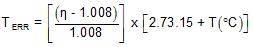
The ideality factor (η) is a measured characteristic of a remote temperature sensor diode as compared to an ideal diode. The ideality factor for the TMP401 is trimmed to be 1.008. For transistors whose ideality factor does not match the TMP401, Equation 1 can be used to calculate the temperature error. Note that for Equation 1 to be used correctly, actual temperature (°C) must be converted to Kelvin (°K).
where
- η = Ideality factor of the remote temperature sensor,
- T(°C) = actual temperature, and
- TERR = Error in the TMP401 reading resulting from η ≠ 1.008. Degree delta is the same for °C and °K.
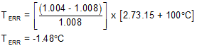
For η = 1.004 and T(°C) = 100°C, use Equation 2:
If a discrete transistor is used as the remote temperature sensor with the TMP401, the best accuracy can be achieved by selecting the transistor according to the following criteria:
- Base-emitter voltage > 0.25 V at 6 μA, at the highest sensed temperature.
- Base-emitter voltage < 0.95 V at 120 μA, at the lowest sensed temperature.
- Base resistance < 100 Ω.
- Tight control of VBE characteristics indicated by small variations in hFE (that is, 50 to 150).
Based on these criteria, two recommended small-signal transistors are the 2N3904 (NPN) or 2N3906 (PNP).
7.4 Device Functional Modes
7.4.1 SMBus Alert Function
The TMP401 supports the SMBus alert function. When pin 6 is configured as an alert output, the ALERT pin of the TMP401 can be connected as an SMBus alert signal. When a master detects an alert condition on the ALERT line, the master sends an SMBus alert command (0001 1001b) on the bus. If the ALERT pin of the TMP401 is active, the devices acknowledge the SMBus alert command and respond by returning its slave address on the SDA line. The eighth bit (LSB) of the slave address byte indicates whether the temperature exceeding one of the temperature high limit settings or falling below one of the temperature low limit settings caused the alert condition. This bit is high if the temperature is greater than or equal to one of the temperature high limit settings; this bit is low if the temperature is less than one of the temperature low limit settings. See Figure 15 for details of this sequence.
If multiple devices on the bus respond to the SMBus alert command, arbitration during the slave address portion of the SMBus alert command determines which device clears its alert status. If the TMP401 wins the arbitration, its ALERT pin becomes inactive at the completion of the SMBus alert command. If the TMP401 loses the arbitration, the ALERT pin remains active.
7.4.2 THERM (Pin 4) and ALERT/THERM2 (Pin 6)
The TMP401 has two pins dedicated to alarm functions, the THERM and ALERT/THERM2 pins. Both pins are open-drain outputs that each require a pull-up resistor to V+. These pins can be wire-ORed together with other alarm pins for system monitoring of multiple sensors. The THERM pin provides a thermal interrupt that cannot be software disabled. The ALERT pin is intended for use as an earlier warning interrupt, and can be software disabled, or masked. The ALERT/THERM2 pin can also be configured for use as THERM2, a second THERM pin (configuration register, AL/TH bit = 1). The default setting configures pin 6 to function as ALERT (AL/TH = 0).
The THERM pin asserts low when either the measured local or remote temperature is outside of the temperature range programmed in the corresponding local and remote THERM limit register. The THERM temperature limit range can be programmed with a wider range than that of the limit registers, which allows ALERT to provide an earlier warning than THERM. The THERM alarm resets automatically when the measured temperature returns to within the THERM temperature limit range minus the hysteresis value stored in the THERM hysteresis register. The allowable values of hysteresis are listed in Table 8. The default hysteresis is 10°C. When the ALERT/THERM2 pin is configured as a second thermal alarm (configuration register, bit 7 = 0, bit 5 = 1), the pin functions the same as THERM, but uses the temperatures stored in the local and remote temperature high and low limit registers to set its comparison range.
When ALERT/THERM2 (pin 6) is configured as ALERT (configuration register, bit 7 = 0, bit 5 = 0), the pin asserts low when either the measured local or remote temperature violates the range limit set by the corresponding local and remote temperature high and low limit registers. This alert function can be configured to assert only if the range is violated a specified number of consecutive times (1, 2, 3, or 4). The consecutive violation limit is set in the consecutive alert register. False alerts that occur as a result of environmental noise can be prevented by requiring consecutive faults. ALERT also asserts low if the remote temperature sensor is open-circuit. When the MASK function is enabled (configuration register, bit 7 = 1), ALERT is disabled (that is, masked). ALERT resets when the master reads the device address, as long as the condition that caused the alert no longer persists, and the status register is reset.
7.4.3 Sensor Fault
The TMP401 senses a fault at the D+ input resulting from incorrect diode connection or an open circuit. The detection circuitry consists of a voltage comparator that trips when the voltage at D+ exceeds (V+) – 0.6 V (typical). The comparator output is continuously checked during a conversion. If a fault is detected, the last valid measured temperature is used for the temperature measurement result, the OPEN bit (status register, bit 2) is set high, and (if the alert function is enabled) ALERT asserts low.
When not using the remote sensor with the TMP401, the D+ and D– inputs must be connected together to prevent meaningless fault warnings.
7.4.4 High-Speed Mode
In order for the two-wire bus to operate at frequencies above 400 kHz, the master device must issue a high-speed mode (Hs-mode) master code (0000 1xxxb) as the first byte after a start condition to switch the bus to high-speed operation. The TMP401 does not acknowledge this byte, but switches the input filters on SDA and SCL and the output filter on SDA to operate in Hs-mode, allowing transfers at up to 2.5 MHz. After the Hs-mode master code is issued, the master transmits a two-wire slave address to initiate a data transfer operation. The bus continues to operate in Hs-mode until a stop condition occurs on the bus. Upon receiving the stop condition, the TMP401 switches the input and output filter back to fast-mode operation.
7.4.5 Shutdown Mode (SD)
The TMP401 shutdown mode (SD) allows the user to save maximum power by shutting down all device circuitry other than the serial interface, thus reducing current consumption to typically less than 3 μA; see Figure 10 (Shutdown Quiescent Current vs Supply Voltage). Shutdown mode is enabled when the SD bit of the configuration register is high; the device shuts down when the current conversion is completed. When SD is low, the device maintains a continuous conversion state.
7.4.6 One-Shot Conversion
When the TMP401 is in shutdown mode (SD = 1 in the configuration register), a single conversion on both channels is started by writing any value to the one-shot start register, pointer address 0Fh. This write operation starts one conversion; the TMP401 returns to shutdown mode when that conversion completes. The value of the data sent in the write command is irrelevant and is not stored by the TMP401. When the TMP401 is set to shutdown mode, an initial 200 μs is required before a one-shot command can be given. This wait time only applies to the 200 μs immediately following shutdown. One-shot commands can be issued without delay thereafter.
7.4.7 General-Call Reset
The TMP401 supports reset via the two-wire general-call address 00h (0000 0000b). The TMP401 acknowledges the general-call address and responds to the second byte. If the second byte is 06h (0000 0110b), the TMP401 executes a software reset. This software reset restores the power-on reset state to all TMP401 registers, aborts any conversion in progress, and clears the ALERT and THERM pins. The TMP401 takes no action in response to other values in the second byte.
7.5 Programming
7.5.1 Bus Overview
The TMP401 is SMBus interface-compatible. In SMBus protocol, the device that initiates the transfer is called a master, and the devices controlled by the master are slaves. The bus must be controlled by a master device that generates the serial clock (SCL), controls the bus access, and generates the start and stop conditions.
To address a specific device, a start condition is initiated. A start condition is indicated by pulling the data line (SDA) from a high to low logic level while SCL is high. All slaves on the bus shift in the slave address byte, with the last bit indicating whether a read or write operation is intended. During the ninth clock pulse, the slave being addressed responds to the master by generating an acknowledge and pulling SDA low.
Data transfer is then initiated and sent over eight clock pulses followed by an acknowledge bit. During data transfer SDA must remain stable while SCL is high, because any change in SDA while SCL is high is interpreted as a control signal.
When all data are transferred, the master generates a stop condition. A stop condition is indicated by pulling SDA from low to high while SCL is high.
7.5.2 Serial Interface
The TMP401 operates only as a slave device on either the two-wire bus or the SMBus. Connections to either bus are made via the open-drain I/O lines, SDA and SCL. The SDA and SCL pins feature integrated spike-suppression filters and Schmitt triggers to minimize the effects of input spikes and bus noise. The TMP401 supports the transmission protocol for fast (1 kHz to 400 kHz) and high-speed (1 kHz to 2.5 MHz) modes. All data bytes are transmitted MSB first.
7.5.3 Serial Bus Address
To communicate with the TMP401, the master must first address slave devices via a slave address byte. The slave address byte consists of seven address bits, and a direction bit indicating the intent of executing a read or write operation. The address of the TMP401 is 4Ch (1001100b).
7.5.4 Read and Write Operations
Accessing a particular register on the TMP401 is accomplished by writing the appropriate value to the pointer register. The value for the pointer register is the first byte transferred after the slave address byte with the R/W bit low. Every write operation to the TMP401 requires a value for the pointer register (see Figure 13).
When reading from the TMP401, the last value stored in the pointer register by a write operation is used to determine which register is read by a read operation. To change the register pointer for a read operation, a new value must be written to the pointer register. This transaction is accomplished by issuing a slave address byte with the R/W bit low, followed by the pointer register byte. No additional data are required. The master can then generate a start condition and send the slave address byte with the R/W bit high to initiate the read command. See Figure 14 for details of this sequence. If repeated reads from the same register are desired, continually sending the pointer register bytes is not necessary, because the TMP401 retains the pointer register value until changed by the next write operation. Note that register bytes are sent MSB first, followed by the LSB.
7.5.5 Timeout Function
When bit 7 of the consecutive alert register is set high, the TMP401 timeout function is enabled. The TMP401 resets the serial interface if either SCL or SDA are held low for 30 ms (typ) between a start and stop condition. If the TMP401 is holding the bus low, the device releases the bus and waits for a start condition. To avoid activating the timeout function, a communication speed of at least 1 kHz must be maintained for the SCL operating frequency. The default state of the timeout function is enabled (bit 7 = high).
7.5.6 Timing Diagrams
The TMP401 is two-wire and SMBus compatible. Figure 12 to Figure 15 describe the various operations on the TMP401. Parameters for Figure 12 are defined in Timing Requirements table. Bus definitions are as follows:
Bus Idle: Both SDA and SCL lines remain high.
Start Data Transfer: A change in the state of the SDA line from high to low while the SCL line is high, defines a start condition. Each data transfer is initiated with a start condition.
Stop Data Transfer: A change in the state of the SDA line from low to high while the SCL line is high defines a stop condition. Each data transfer terminates with a repeated start or stop condition.
Data Transfer: The number of data bytes transferred between a start and a stop condition is not limited and is determined by the master device. The receiver acknowledges the transfer of data.
Acknowledge: Each receiving device, when addressed, is obliged to generate an acknowledge bit. A device that acknowledges must pull down the SDA line during the acknowledge clock pulse in such a way that the SDA line is stable low during the high period of the acknowledge clock pulse. Setup and hold times must be taken into account. On a master receive, data transfer termination can be signaled by the master generating a not-acknowledge on the last byte transmitted by the slave.
 Figure 12. Two-Wire Timing Diagram
 Figure 13. Two-Wire Timing Diagram for Write Word Format
 Figure 14. Two-Wire Timing Diagram for Read Word Format
 Figure 15. Timing Diagram for SMBus Alert
7.6 Register Maps
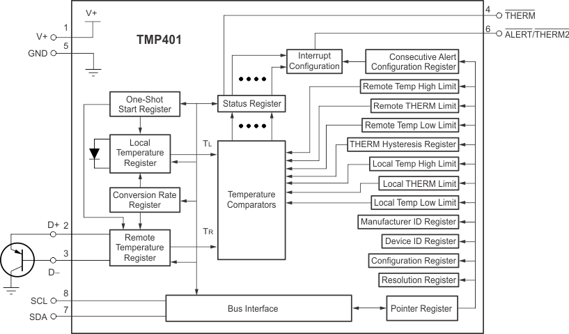
The TMP401 contains multiple registers for holding configuration information, temperature measurement results, temperature comparator limits, and status information. These registers are described in Figure 16 and Table 3.
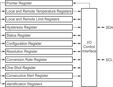 Figure 16. Internal Register Structure
Table 3. Register Map
7.6.1 Pointer Register
Figure 16 illustrates the internal register structure of the TMP401. The 8-bit pointer register is used to address a given data register. The pointer register identifies which of the data registers respond to a read or write command on the two-wire bus. This register is set with every write command. A write command must be issued to set the proper value in the pointer register before executing a read command. Table 3 describes the pointer address of the registers available in the TMP401. The power-on reset (POR) value of the pointer register is 00h (0000 0000b).
7.6.2 Temperature Registers
The TMP401 has four 8-bit registers that hold temperature measurement results. Both the local channel and the remote channel have a high byte register that contains the most significant bits (MSBs) of the temperature ADC result and a low byte register that contains the least significant bits (LSBs) of the temperature ADC result. The local channel high byte address is 00h; the local channel low byte address is 15h. The remote channel high byte is at address 01h; the remote channel low byte address is 10h. These registers are read-only and are updated by the ADC each time a temperature measurement is completed.
The TMP401 contains circuitry to assure that a low byte register read command returns data from the same ADC conversion as the immediately preceding high byte read command. This assurance remains valid only until another register is read. For proper operation, the high byte of a temperature register must be read first. Read the low byte register in the next read command. The low byte register may be left unread if the LSBs are not needed. Alternatively, the temperature registers can be read as a 16-bit register by using a single two-byte read command from address 00h for the local channel result or from address 01h for the remote channel result. The high byte is output first, followed by the low byte. Both bytes of this read operation are from the same ADC conversion. The power-on reset value of both temperature registers is 00h.
7.6.3 Limit Registers
The TMP401 has 11 registers for setting comparator limits for both the local and remote measurement channels. These registers have read and write capability. The high and low limit registers for both channels span two registers, as do the temperature registers. The local temperature high limit is set by writing the high byte to pointer address 0Bh and writing the low byte to pointer address 16h, or by using a single two-byte write command (high byte first) to pointer address 0Bh. The local temperature high limit is obtained by reading the high byte from pointer address 05h and the low byte from pointer address 16h, or by using a two-byte read command from pointer address 05h. The power-on reset value of the local temperature high limit is 55h, standard, and 00h, extended (+85°C in standard temperature mode; +21°C in extended temperature mode).
Similarly, the local temperature low limit is set by writing the high byte to pointer address 0Ch and writing the low byte to pointer address 17h, or by using a single two-byte write command to pointer address 0Ch. The local temperature low limit is read by reading the high byte from pointer address 06h and the low byte from pointer address 17h, or by using a two-byte read from pointer address 06h. The power-on reset value of the local temperature low limit register is 00h, standard and extended (0°C in standard temperature mode; –64°C in extended mode).
The remote temperature high limit is set by writing the high byte to pointer address 0Dh and writing the low byte to pointer address 13h, or by using a two-byte write command to pointer address 0Dh. The remote temperature high limit is obtained by reading the high byte from pointer address 07h and the low byte from pointer address 13h, or by using a two-byte read command from pointer address 07h. The power-on reset value of the remote temperature high limit register is 55h, standard, and 00h, extended (+85°C in standard temperature mode; +21°C in extended temperature mode).
The remote temperature low limit is set by writing the high byte to pointer address 0Eh and writing the low byte to pointer address 14h, or by using a two-byte write to pointer address 0Eh. The remote temperature low limit is read by reading the high byte from pointer address 08h and the low byte from pointer address 14h, or by using a two-byte read from pointer address 08h. The power-on reset value of the remote temperature low limit register is 00h, standard and extended (0°C in standard temperature mode; –64°C in extended mode).
The TMP401 also has a THERM limit register for both the local and the remote channels. These registers are eight bits and allow for THERM limits set to 1°C resolution. The local channel THERM limit is set by writing to pointer address 20h. The remote channel THERM limit is set by writing to pointer address 19h. The local channel THERM limit is obtained by reading from pointer address 20h; the remote channel THERM limit is read by reading from pointer address 19h. The power-on reset value of the THERM limit registers is 55h (+85°C in standard temperature mode; +21°C in extended temperature mode). The THERM limit comparators also have hysteresis. The hysteresis of both comparators is set by writing to pointer address 21h. The hysteresis value is obtained by reading from pointer address 21h. The value in the hysteresis register is an unsigned number (always positive). The power-on reset value of this register is 0Ah (+10°C).
Whenever changing between standard and extended temperature ranges, be aware that the temperatures stored in the temperature limit registers are not automatically reformatted to correspond to the new temperature range format. These values must be reprogrammed in the appropriate binary or extended binary format.
7.6.4 Status Register
The TMP401 has a status register to report the state of the temperature comparators. Figure 17 shows the status register bits. The status register is read-only and is read by reading from pointer address 02h.
| D7 | D6 | D5 | D4 | D3 | D2 | D1 | D0 |
| BUSY(1) | LHIGH | LLOW | RHIGH | RLOW | OPEN | RTHRM | LTHRM |
| R-0b | R-0b | R-0b | R-0b | R-0b | R-0b | R-0b | R-0b |
| LEGEND: R = Read only; -n = value after reset |
The BUSY bit reads as ‘1’ if the ADC is making a conversion. It reads as ‘0’ if the ADC is not converting.
The OPEN bit reads as ‘1’ if the remote transistor is detected as open from the last read of the status register. The OPEN status is only detected when the ADC is attempting to convert a remote temperature.
The RTHRM bit reads as ‘1’ if the remote temperature exceeds the remote THERM limit and remains greater than the remote THERM limit less the value in the shared hysteresis register, as shown in Figure 18.
The LTHRM bit reads as ‘1’ if the local temperature exceeds the local THERM limit and remains greater than the local THERM limit less the value in the shared hysteresis register, as shown in Figure 18.
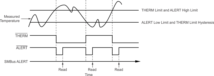 Figure 18. SMBus Alert Timing Diagram
The LHIGH and RHIGH bit values depend on the state of the AL/TH bit in the configuration register. If the AL/TH bit is ‘0’, the LHIGH bit reads as ‘1’ if the local high limit is exceeded from the last clearing of the status register. The RHIGH bit reads as ‘1’ if the remote high limit is exceeded from the last clearing of the status register. If the AL/TH bit is ‘1’, the remote high limit and the local high limit are used to implement a THERM2 function. LHIGH reads as ‘1’ if the local temperature exceeds the local high limit and remains greater than the local high limit less the value in the hysteresis register.
The RHIGH bit reads as ‘1’ if the remote temperature exceeds the remote high limit and remains greater than the remote high limit less the value in the hysteresis register.
The LLOW and RLOW bits are not affected by the AL/TH bit. The LLOW bit reads as ‘1’ if the local low limit is exceeded from the last clearing of the status register. The RLOW bit reads as ‘1’ if the remote low limit is exceeded from the last clearing of the status register.
The values of the LLOW, RLOW, and OPEN (as well as LHIGH and RHIGH when AL/TH is ‘0’) are latched and read as ‘1’ until the status register is read or a device reset occurs. These bits are cleared by reading the status register, provided that the condition causing the flag to be set no longer exists. The values of BUSY, LTHRM, and RTHRM (as well as LHIGH and RHIGH when AL/TH is ‘1’) are not latched and are not cleared by reading the status register. These bits always indicate the current state, and are updated appropriately at the end of the corresponding ADC conversion. Clearing the status register bits does not clear the state of the ALERT pin; an SMBus alert response address command must be used to clear the ALERT pin.
The TMP401 NORs LHIGH, LLOW, RHIGH, RLOW, and OPEN, so a status change for any of these flags from ‘0’ to ‘1’ automatically causes the ALERT pin to go low (only applies when the ALERT/THERM2 pin is configured for ALERT mode).
7.6.5 Configuration Register
The configuration register sets the temperature range, controls shutdown mode, and determines how the ALERT/THERM2 pin functions. The configuration register is set by writing to pointer address 09h and read by reading from pointer address 03h.
The MASK bit (bit 7) enables or disables the ALERT pin output if AL/TH = 0. If AL/TH = 1, then the MASK bit has no effect. If MASK is set to ‘0’, the ALERT pin goes low when one of the temperature measurement channels exceeds its high or low limits for the chosen number of consecutive conversions. If the MASK bit is set to ‘1’, the TMP401 retains the ALERT pin status, but the ALERT pin does not go low.
The shutdown (SD) bit (bit 6) enables or disables the temperature measurement circuitry. If SD = 0, the TMP401 converts continuously at the rate set in the conversion rate register. When SD is set to ‘1’, the TMP401 immediately stops converting and enters a shutdown mode. When SD is set to ‘0’ again, the TMP401 resumes continuous conversions. A single conversion can be started when SD = 1 by writing to the one-shot register.
The AL/TH bit (bit 5) controls whether the ALERT pin functions in ALERT mode or THERM2 mode. If AL/TH = 0, the ALERT pin operates as an interrupt pin. In this mode, the ALERT pin goes low after the set number of consecutive out-of-limit temperature measurements occur.
If AL/TH = 1, the ALERT/THERM2 pin implements a THERM function (THERM2). In this mode, THERM2 functions similar to the THERM pin except that the local high limit and remote high limit registers are used for the thresholds. THERM2 goes low when either RHIGH or LHIGH is set.
The temperature range is set by configuring bit 2 of the configuration register. Setting this bit low configures the TMP401 for the standard measurement range (0°C to +127°C); temperature conversions are stored in standard binary format. Setting bit 2 high configures the TMP401 for the extended measurement range (–55°C to +150°C); temperature conversions are stored in extended binary format (see Table 1).
The remaining bits of the configuration register are reserved and must always be set to ‘0’. The power-on reset value for this register is 00h. Figure 19 and Table 4 summarize the bits of the configuration register.
| D7 | D6 | D5 | D4 | D3 | D2 | D1 | D0 |
| MASK | SD | AL/TH | Reserved | Reserved | Temperature Range | Reserved | Reserved |
| R/W-0 | R/W-0 | R/W-0 | — | — | R/W-0 | — | — |
| LEGEND: R/W = Read/Write; R = Read only; -n = value after reset |
Table 4. Configuration Register Field Descriptions
| Bit | Field | Type | Reset | Description |
|---|---|---|---|---|
| D7 | MASK | R/W | 0 | 0 = ALERT Enabled 1 = ALERT Masked |
| D6 | SD | R/W | 0 | 0 = Run 1 = Shut Down |
| D5 | AL/TH | R/W | 0 | 0 = ALERT Mode 1 = THERM Mode |
| D[4:3] | Reserved | — | — | — |
| D2 | Temperature Range | R/W | 0 | 0 = 0°C to +127°C 1 = –55°C to +150°C |
| D[1:0] | Reserved | — | — | — |
7.6.6 Resolution Register
The RES1 and RES0 bits (resolution bits 1 and 0) of the resolution register set the resolution of the local temperature measurement channel. Remote temperature measurement channel resolution is not affected. Changing the local channel resolution also affects the conversion time and rate of the TMP401. The resolution register is set by writing to pointer address 1Ah and is read by reading from pointer address 1Ah. Figure 20 and Table 5 show the resolution bits for the resolution register.
Bits 2 through 4 of the resolution register must always be set to ‘1’. Bits 5 through 7 of the resolution register must always be set to ‘0’. The power-on reset value of this register is 1Ch.
| D7 | D6 | D5 | D4 | D3 | D2 | D1 | D0 |
| 0 | 0 | 0 | 1 | 1 | 1 | RES1 | RES0 |
| R-0b | R-0b | R-0b | R-1b | R-1b | R-1b | R/W-0b | R/W-0b |
| LEGEND: R/W = Read/Write; R = Read only; -n = value after reset |
Table 5. Resolution Register: Local Channel Programmable Resolution
| RES1 | RES0 | RESOLUTION | CONVERSION TIME (Typical) |
|---|---|---|---|
| 0 | 0 | 9 Bits (0.5°C) | 12.5 ms |
| 0 | 1 | 10 Bits (0.25°C) | 25 ms |
| 1 | 0 | 11 Bits (0.125°C) | 50 ms |
| 1 | 1 | 12 Bits (0.0625°C) | 100 ms |
7.6.7 Conversion Rate Register
The conversion rate register controls the rate at which temperature conversions are performed. This register adjusts the idle time between conversions but not the conversion timing itself, thereby allowing the TMP401 power dissipation to be balanced with the temperature register update rate. Figure 21 shows the conversion rate register bits and Table 6 shows the conversion rate options and corresponding current consumption.
| D7 | D6 | D5 | D4 | D3 | D2 | D1 | D0 |
| 0 | 0 | 0 | 0 | R3 | R2 | R1 | R0 |
| R-0b | R-0b | R-0b | R-0b | R/W-1b | R/W-0b | R/W-0b | R/W-0b |
| LEGEND: R/W = Read/Write; R = Read only; -n = value after reset |
Table 6. Conversion Rate Register
7.6.8 Identification Registers
The TMP401 allows for the two-wire bus controller to query the device for manufacturer and device IDs to allow for software identification of the device at the particular two-wire bus address. The manufacturer ID is obtained by reading from pointer address FEh. The device ID is obtained by reading from pointer address FFh. The TMP401 returns 55h for the manufacturer code and 11h for the device ID. These registers are read-only.
7.6.9 Consecutive Alert Register
The value in the consecutive alert register (address 22h) determines how many consecutive out-of-limit measurements must occur on a measurement channel before the ALERT signal is activated. The value in this register does not affect bits in the status register. Values of one, two, three, or four consecutive conversions can be selected; one conversion is the default. This function allows additional filtering for the ALERT pin. Figure 22 lists the consecutive alert register bits. The consecutive alert bits are shown in Table 7.
| D7 | D6 | D5 | D4 | D3 | D2 | D1 | D0 |
| TO_EN | 0 | 0 | 0 | C2 | C1 | C0 | 1 |
| R/W-1b | R-0b | R-0b | R-0b | R/W-0b | R/W-0b | R/W-0b | R-1b |
| LEGEND: R/W = Read/Write; R = Read only; -n = value after reset |
Table 7. Consecutive Alert Register
| C2 | C1 | C0 | NUMBER OF CONSECUTIVE OUT-OF-LIMIT MEASUREMENTS |
|---|---|---|---|
| 0 | 0 | 0 | 1 |
| 0 | 0 | 1 | 2 |
| 0 | 1 | 1 | 3 |
| 1 | 1 | 1 | 4 |
NOTE
Bit 7 of the consecutive alert register controls the enable and disable of the timeout function. See the Timeout Function section for a description of this feature.
7.6.10 THERM Hysteresis Register
The THERM hysteresis register stores the hysteresis value used for the THERM pin alarm function. This register must be programmed with a value that is less than the local temperature high limit register value, remote temperature high limit register value, local THERM limit register value, or remote THERM limit register value; otherwise, the respective temperature comparator does not trip on the measured temperature falling edges. Figure 23 lists the THERM hysteresis register bits. Allowable hysteresis values are shown in Table 8. The default hysteresis value is 10°C, whether the device is operating in the standard or extended mode setting.
| D7 | D6 | D5 | D4 | D3 | D2 | D1 | D0 |
| TH11 | TH10 | TH9 | TH8 | TH7 | TH6 | TH5 | TH4 |
| R/W-0h | R/W-0h | R/W-0h | R/W-0h | R/W-1h | R/W-0h | R/W-1h | R/W-0h |
| LEGEND: R/W = Read/Write; -n = value after reset |
Table 8. Allowable THERM Hysteresis Values
| TEMPERATURE (°C) | THERM HYSTERESIS VALUE | |
|---|---|---|
| TH[11:4] (Standard Binary) | HEXADECIMAL | |
| 0 | 0000 0000 | 00 |
| 1 | 0000 0001 | 01 |
| 5 | 0000 0101 | 05 |
| 10 | 0000 1010 | 0A |
| 25 | 0001 1001 | 19 |
| 50 | 0011 0010 | 32 |
| 75 | 0100 1011 | 4B |
| 100 | 0110 0100 | 64 |
| 125 | 0111 1101 | 7D |
| 127 | 0111 1111 | 7F |
| 150 | 1001 0110 | 96 |
| 175 | 1010 1111 | AF |
| 200 | 1100 1000 | C8 |
| 225 | 1110 0001 | E1 |
| 255 | 1111 1111 | FF |