SBOS371B August 2006 – October 2014 TMP401
PRODUCTION DATA.
- 1 Features
- 2 Applications
- 3 Description
- 4 Revision History
- 5 Pin Configuration and Functions
- 6 Specifications
- 7 Detailed Description
- 8 Application and Implementation
- 9 Power-Supply Recommendations
- 10Layout
- 11Device and Documentation Support
- 12Mechanical, Packaging, and Orderable Information
Package Options
Mechanical Data (Package|Pins)
- DGK|8
Thermal pad, mechanical data (Package|Pins)
Orderable Information
10 Layout
10.1 Layout Guidelines
10.1.1 Measurement Accuracy and Thermal Considerations
The temperature measurement accuracy of the TMP401 depends on the remote and local temperature sensor being at the same temperature as the system point being monitored. Clearly, if the temperature sensor is not in good thermal contact with the part of the system being monitored, then there is a delay in the response of the sensor to a temperature change in the system. For remote temperature sensing applications using a substrate transistor (or a small, SOT23 transistor) placed close to the device being monitored, this delay is usually not a concern.
The local temperature sensor inside the TMP401 monitors the ambient air around the device. The thermal time constant for the TMP401 is approximately two seconds. This constant implies that if the ambient air changes quickly by 100°C, the TMP401 takes approximately 10 seconds (that is, five thermal time constants) to settle to within 1°C of the final value. In most applications, the TMP401 package is in electrical and therefore thermal contact with the PCB, as well as subjected to forced airflow. The accuracy of the measured temperature directly depends on how accurately the PCB and forced airflow temperatures represent the temperature that the TMP401 is measuring. Additionally, the internal power dissipation of the TMP401 can cause the temperature to rise above the ambient or PCB temperature. The internal power dissipated as a result of exciting the remote temperature sensor is negligible because of the small currents used. For a 5.5-V supply and maximum conversion rate of eight conversions per second, the TMP401 dissipates 1.82 mW (PDIQ = 5.5 V × 330 µA). If both the ALERT/THERM2 and THERM pins are each sinking 1 mA, an additional power of 0.8 mW is dissipated (PDOUT = 1 mA × 0.4 V + 1 mA × 0.4 V = 0.8 mW). Total power dissipation is then 2.62 mW (PDIQ + PDOUT) and, with a θJA of 78.8°C/W, causes the junction temperature to rise approximately 0.206°C above the ambient.
10.1.2 Layout Considerations
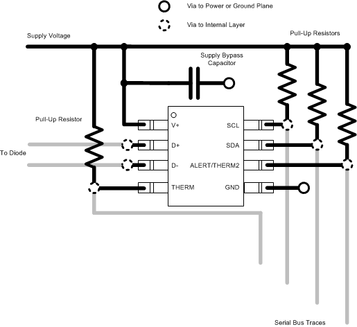
Remote temperature sensing on the TMP401 measures very small voltages using very small currents; therefore, noise at the IC inputs must be minimized. Most applications using the TMP401 have high digital content, with several clocks and logic level transitions creating a noisy environment. Layout must adhere to the following guidelines:
- Place the TMP401 as close to the remote junction sensor as possible.
- Route the D+ and D– traces next to each other and shield them from adjacent signals through the use of ground guard traces; see Figure 28. If a multilayer PCB is used, bury these traces between ground or VDD planes to shield them from extrinsic noise sources. 5-mil PCB traces are recommended.
- Minimize additional thermocouple junctions caused by copper-to-solder connections. If these junctions are used, make the same number and approximate locations of copper-to-solder connections in both the D+ and D– connections to cancel any thermocouple effects; see Figure 30.
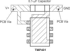
- Use a 0.1-μF local bypass capacitor directly between the V+ and GND of the TMP401; see Figure 29. Minimize filter capacitance between D+ and D– to 1000 pF or less for optimum measurement performance. This capacitance includes any cable capacitance between the remote temperature sensor and the TMP401.
- If the connection between the remote temperature sensor and the TMP401 is between 8 inches and 12 feet, use a twisted-wire pair connection. Beyond this distance (up to 100 ft), use a twisted, shielded pair with the shield grounded as close to the TMP401 as possible. Leave the remote sensor connection end of the shield wire open to avoid ground loops and 60-Hz pickup.
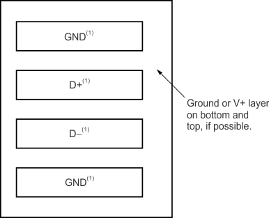 Figure 28. Example Signal Traces