SBOS371B August 2006 – October 2014 TMP401
PRODUCTION DATA.
- 1 Features
- 2 Applications
- 3 Description
- 4 Revision History
- 5 Pin Configuration and Functions
- 6 Specifications
- 7 Detailed Description
- 8 Application and Implementation
- 9 Power-Supply Recommendations
- 10Layout
- 11Device and Documentation Support
- 12Mechanical, Packaging, and Orderable Information
Package Options
Mechanical Data (Package|Pins)
- DGK|8
Thermal pad, mechanical data (Package|Pins)
Orderable Information
5 Pin Configuration and Functions
DGK Package
VSSOP-8
(Top View)
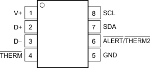
Pin Functions
| PIN | I/O | DESCRIPTION | |
|---|---|---|---|
| NO. | NAME | ||
| 1 | V+ | Analog input | Positive supply (3 V to 5.5 V) |
| 2 | D+ | Analog input | Positive connection to remote temperature sensor |
| 3 | D– | Analog input | Negative connection to remote temperature sensor |
| 4 | THERM | Digital output | Thermal flag, active low, open-drain; requires pull-up resistor to V+ |
| 5 | GND | — | Ground |
| 6 | ALERT/THERM2 | Digital output | Alert (reconfigurable as second thermal flag), active low, open-drain; requires pull-up resistor to V+ |
| 7 | SDA | Digital I/O | Serial data line for SMBus, open-drain; requires pull-up resistor to V+ |
| 8 | SCL | Digital I/O | Serial clock line for SMBus, open-drain; requires pull-up resistor to V+ |