SLOS877C October 2014 – April 2021 TMP451-Q1
PRODUCTION DATA
- 1 Features
- 2 Applications
- 3 Description
- 4 Revision History
- 5 Pin Configuration and Functions
- 6 Specifications
-
7 Detailed Description
- 7.1 Overview
- 7.2 Functional Block Diagram
- 7.3 Feature Description
- 7.4 Device Functional Modes
- 7.5 Programming
- 7.6 Register Map
- 8 Application and Implementation
- 9 Power Supply Recommendations
- 10Layout
- 11Device and Documentation Support
- 12Mechanical, Packaging, and Orderable Information
Package Options
Mechanical Data (Package|Pins)
Thermal pad, mechanical data (Package|Pins)
Orderable Information
7.6.1.7 η-Factor Correction Register
The TMP451-Q1 device allows for a different η-factor value to be used for converting remote channel measurements to temperature. The remote channel uses sequential current excitation to extract a differential VBE voltage measurement to determine the temperature of the remote transistor. Equation 1 shows this voltage and temperature.
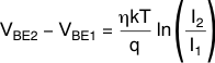
The value η in Equation 1 is a characteristic of the particular transistor used for the remote channel. The power-on reset value for the TMP451-Q1 device is η = 1.008. The value in the η-factor correction register may be used to adjust the effective η-factor according to Equation 2 and Equation 3.
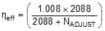

The η-factor correction value must be stored in twos complement format, yielding an effective data range from –128 to 127. The η-factor correction value is written to and read from pointer address 23h. The register power-on reset value is 00h, thus having no effect unless a different value is written to it.
| NADJUST | η | ||
|---|---|---|---|
| BINARY | HEX | DECIMAL | |
| 0111 1111 | 7F | 127 | 0.950198 |
| 0000 1010 | 0A | 10 | 1.003195 |
| 0000 1000 | 08 | 8 | 1.004152 |
| 0000 0110 | 06 | 6 | 1.005111 |
| 0000 0100 | 04 | 4 | 1.006072 |
| 0000 0010 | 02 | 2 | 1.007035 |
| 0000 0001 | 01 | 1 | 1.007517 |
| 0000 0000 | 00 | 0 | 1.008 |
| 1111 1111 | FF | –1 | 1.008483 |
| 1111 1110 | FE | –2 | 1.008967 |
| 1111 1100 | FC | –4 | 1.009935 |
| 1111 1010 | FA | –6 | 1.010905 |
| 1111 1000 | F8 | –8 | 1.011877 |
| 1111 0110 | F6 | –10 | 1.012851 |
| 1000 0000 | 80 | –128 | 1.073837 |