SBOS583B December 2011 – December 2016 TMP709
PRODUCTION DATA.
- 1 Features
- 2 Applications
- 3 Description
- 4 Revision History
- 5 Pin Configuration and Functions
- 6 Specifications
- 7 Detailed Description
- 8 Applications and Implementation
- 9 Power Supply Recommendations
- 10Layout
- 11Device and Documentation Support
- 12Mechanical, Packaging, and Orderable Information
Package Options
Mechanical Data (Package|Pins)
- DBV|5
Thermal pad, mechanical data (Package|Pins)
Orderable Information
8 Applications and Implementation
NOTE
Information in the following applications sections is not part of the TI component specification, and TI does not warrant its accuracy or completeness. TI’s customers are responsible for determining suitability of components for their purposes. Customers should validate and test their design implementation to confirm system functionality.
8.1 Application Information
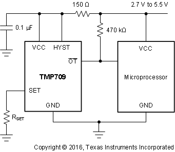
The TMP709 device is simple to configure. The only external components that the device requires are a bypass capacitor and pullup resistor. Power-supply bypassing is strongly recommended. Use a 0.1-µF capacitor placed as close as possible to the VCC supply pin. To minimize the internal power dissipation of the TMP709 family of devices, use a pullup resistor value greater than 10 kΩ from the OT pin to the VCC pin. See the Hysteresis Input section for hysteresis configuration, and the Set-Point Resistor (RSET) section for configuring the temperature threshold.
8.2 Typical Application
 Figure 5. Overtemperature Protection for a 60°C Trip Point
8.2.1 Design Requirements
For this design example, a 2.7-V to 5.5-V power supply, 60°C trip point, and 10°C hysteresis are used.
8.2.2 Detailed Design Procedure
Connect the HYST pin to VCC for 10°C hysteresis. For a 60°C temperature threshold, see the Set-Point Resistor (RSET) section to compute an ideal RSET resistor value of 44.619 kΩ. Select the closest standard value resistor available; in this case, 44.2 kΩ. Use a 10-kΩ pullup resistor from the OT pin to the VCC pin. To minimize power, a larger-value pullup resistor can be used, but must not exceed 470 kΩ. Place a 0.1-μF bypass capacitor close to the TMP709 device in order to reduce noise coupled from the power supply.
8.2.3 Application Curves
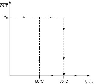
Figure 6 shows an example of the hysteresis feature. The HYST pin is connected to VCC, so the TMP709 device is configured for 10°C of hysteresis. The device is configured for a 60°C trip temperature by the RSET resistor value; therefore, the OT output asserts low when the 60°C threshold is exceeded. The OT output remains asserted low until the sensor reaches 50°C.
 Figure 6. TMP709 Hysteresis Function