SBOS706B April   2014  – August 2014 TMP75B

PRODUCTION DATA.  

  1. Features
  2. Applications
  3. Description
  4. Revision History
  5. Pin Configuration and Functions
  6. Specifications
    1. 6.1 Absolute Maximum Ratings
    2. 6.2 Handling Ratings
    3. 6.3 Recommended Operating Conditions
    4. 6.4 Thermal Information
    5. 6.5 Electrical Characteristics
    6. 6.6 Typical Characteristics
  7. Detailed Description
    1. 7.1 Overview
    2. 7.2 Functional Block Diagram
    3. 7.3 Feature Description
      1. 7.3.1 Digital Temperature Output
      2. 7.3.2 Temperature Limits and Alert
      3. 7.3.3 Serial Interface
        1. 7.3.3.1  Bus Overview
        2. 7.3.3.2  Serial Bus Address
        3. 7.3.3.3  Writing and Reading Operation
        4. 7.3.3.4  Slave-Mode Operations
          1. 7.3.3.4.1 Slave Receiver Mode:
          2. 7.3.3.4.2 Slave Transmitter Mode:
        5. 7.3.3.5  SMBus Alert Function
        6. 7.3.3.6  General Call
        7. 7.3.3.7  High-Speed (Hs) Mode
        8. 7.3.3.8  Timeout Function
        9. 7.3.3.9  Two-Wire Timing
        10. 7.3.3.10 Two-Wire Timing Diagrams
    4. 7.4 Device Functional Modes
      1. 7.4.1 Continuous-Conversion Mode
      2. 7.4.2 Shutdown Mode
      3. 7.4.3 One-Shot Mode
    5. 7.5 Programming
    6. 7.6 Register Map
  8. Application and Implementation
    1. 8.1 Application Information
    2. 8.2 Typical Application
      1. 8.2.1 Design Requirements
      2. 8.2.2 Detailed Design Procedure
      3. 8.2.3 Application Curves
  9. Power Supply Recommendations
  10. 10Layout
    1. 10.1 Layout Guidelines
    2. 10.2 Layout Example
  11. 11Device and Documentation Support
    1. 11.1 Documentation Support
      1. 11.1.1 Related Documentation
    2. 11.2 Trademarks
    3. 11.3 Electrostatic Discharge Caution
    4. 11.4 Glossary
  12. 12Mechanical, Packaging, and Orderable Information

Package Options

Mechanical Data (Package|Pins)
Thermal pad, mechanical data (Package|Pins)
Orderable Information

10 Layout

10.1 Layout Guidelines

Place the power-supply bypass capacitor as close as possible to the supply and ground pins. The recommended value of this bypass capacitor is 0.01 μF. Additional decoupling capacitance can be added to compensate for noisy or high-impedance power supplies.

Pull up the open-drain output pins (SDA and ALERT) to a supply voltage rail (VS or higher but up to 3.6 V) through 10-kΩ pull-up resistors.

10.2 Layout Example

ai_recommended_layout_sbos706.gif
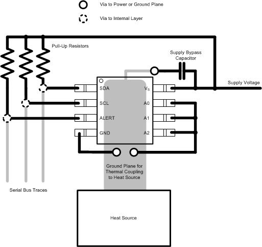
Figure 21. Layout Example