SBOS706B April 2014 – August 2014 TMP75B
PRODUCTION DATA.
- 1 Features
- 2 Applications
- 3 Description
- 4 Revision History
- 5 Pin Configuration and Functions
- 6 Specifications
-
7 Detailed Description
- 7.1 Overview
- 7.2 Functional Block Diagram
- 7.3
Feature Description
- 7.3.1 Digital Temperature Output
- 7.3.2 Temperature Limits and Alert
- 7.3.3 Serial Interface
- 7.4 Device Functional Modes
- 7.5 Programming
- 7.6 Register Map
- 8 Application and Implementation
- 9 Power Supply Recommendations
- 10Layout
- 11Device and Documentation Support
- 12Mechanical, Packaging, and Orderable Information
Package Options
Mechanical Data (Package|Pins)
Thermal pad, mechanical data (Package|Pins)
Orderable Information
5 Pin Configuration and Functions
D and DGK Packages
SOIC-8 and VSSOP-8
(Top View)
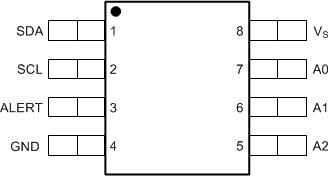
Pin Functions
| PIN | I/O | DESCRIPTION | |
|---|---|---|---|
| NAME | NO. | ||
| A0 | 7 | I | Address select. Connect to GND or VS. |
| A1 | 6 | I | Address select. Connect to GND or VS. |
| A2 | 5 | I | Address select. Connect to GND or VS. |
| ALERT | 3 | O | Overtemperature alert. Open-drain output; requires a pull-up resistor. |
| GND | 4 | — | Ground. |
| SCL | 2 | I | Serial clock. |
| SDA | 1 | I/O | Serial data. Open-drain output; requires a pull-up resistor. |
| VS | 8 | I | Supply voltage, 1.4 V to 3.6 V. |