SBOSA26A December 2020 – February 2021 TMP9A00-EP
PRODUCTION DATA
- 1 Features
- 2 Applications
- 3 Description
- 4 Revision History
- 5 Pin Configuration and Functions
- 6 Specifications
- 7 Detailed Description
- 8 Application and Implementation
- 9 Power Supply Recommendations
- 10Layout
- 11Device and Documentation Support
- 12Introduction to Mechanical, Packaging, and Orderable Information
Package Options
Mechanical Data (Package|Pins)
- DCK|5
Thermal pad, mechanical data (Package|Pins)
Orderable Information
3 Description
The TMP9A00-EP device is a CMOS, precision analog output temperature sensor available in a tiny 5-pin SC70 package. The TMP9A00-EP operates from –55 °C to 150 °C on a supply voltage of 1.8 V to 5.5 V with a supply current of 4 µA. Operation as low as 1.8 V is possible for temperatures between 15 °C and 150 °C. The linear transfer function has a slope of –11.77 mV/°C (typical) and an output voltage of 1.8639 V (typical) at 0 °C. The TMP9A00-EP has a ±2.5 °C accuracy a from –55 °C to 130 °C and ±3.5 °C from 130 °C to 150 °C.
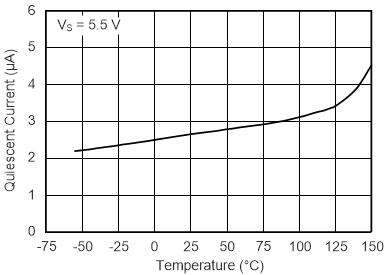
The 4-µA (maximum) supply current of the TMP9A00-EP limits self-heating of the device to less than 0.01 °C. When V+ is less than 0.5 V, the device is in shutdown mode and consumes less than 20 nA (typical).
The TMP9A00-EP is available in a 5-pin SC70 package that reduces the overall required board space.
| PART NUMBER | PACKAGE | BODY SIZE (NOM) |
|---|---|---|
| TMP9A00-EP | SC70 (5) | 2.00 mm × 1.25 mm |
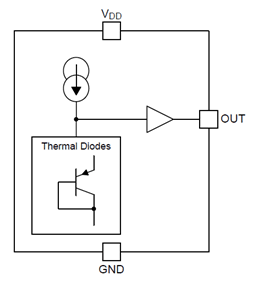
 Device Block Diagram
 Device Quiescent Current Over Temperature