SPRS797F November   2012  – September 2021 TMS320F28050 , TMS320F28051 , TMS320F28052 , TMS320F28052F , TMS320F28052M , TMS320F28053 , TMS320F28054 , TMS320F28054F , TMS320F28054M , TMS320F28055

PRODUCTION DATA  

  1. Features
  2. Applications
  3. Description
    1. 3.1 Functional Block Diagram
  4. Revision History
  5. Device Comparison
    1. 5.1 Related Products
  6. Terminal Configuration and Functions
    1. 6.1 Pin Diagram
    2. 6.2 Signal Descriptions
      1. 6.2.1 Signal Descriptions
  7. Specifications
    1. 7.1  Absolute Maximum Ratings
    2. 7.2  ESD Ratings – Commercial
    3. 7.3  ESD Ratings – Automotive
    4. 7.4  Recommended Operating Conditions
    5. 7.5  Power Consumption Summary
      1. 7.5.1 TMS320F2805x Current Consumption at 60-MHz SYSCLKOUT
      2. 7.5.2 Reducing Current Consumption
      3. 7.5.3 Current Consumption Graphs (VREG Enabled)
    6. 7.6  Electrical Characteristics
    7. 7.7  Thermal Resistance Characteristics for PN Package
    8. 7.8  Thermal Design Considerations
    9. 7.9  JTAG Debug Probe Connection Without Signal Buffering for the MCU
    10. 7.10 Parameter Information
      1. 7.10.1 Timing Parameter Symbology
      2. 7.10.2 General Notes on Timing Parameters
    11. 7.11 Test Load Circuit
    12. 7.12 Power Sequencing
      1. 7.12.1 Reset ( XRS) Timing Requirements
      2. 7.12.2 Reset ( XRS) Switching Characteristics
    13. 7.13 Clock Specifications
      1. 7.13.1 Device Clock Table
        1. 7.13.1.1 2805x Clock Table and Nomenclature (60-MHz Devices)
        2. 7.13.1.2 Device Clocking Requirements/Characteristics
        3. 7.13.1.3 Internal Zero-Pin Oscillator (INTOSC1, INTOSC2) Characteristics
      2. 7.13.2 Clock Requirements and Characteristics
        1. 7.13.2.1 XCLKIN Timing Requirements - PLL Enabled
        2. 7.13.2.2 XCLKIN Timing Requirements - PLL Disabled
        3. 7.13.2.3 XCLKOUT Switching Characteristics (PLL Bypassed or Enabled)
    14. 7.14 Flash Timing
      1. 7.14.1 Flash/OTP Endurance for T Temperature Material
      2. 7.14.2 Flash/OTP Endurance for S Temperature Material
      3. 7.14.3 Flash/OTP Endurance for Q Temperature Material
      4. 7.14.4 Flash Parameters at 60-MHz SYSCLKOUT
      5. 7.14.5 Flash/OTP Access Timing
      6. 7.14.6 Flash Data Retention Duration
  8. Detailed Description
    1. 8.1 Overview
      1. 8.1.1  CPU
      2. 8.1.2  Control Law Accelerator
      3. 8.1.3  Memory Bus (Harvard Bus Architecture)
      4. 8.1.4  Peripheral Bus
      5. 8.1.5  Real-Time JTAG and Analysis
      6. 8.1.6  Flash
      7. 8.1.7  M0, M1 SARAMs
      8. 8.1.8  L0 SARAM, and L1, L2, and L3 DPSARAMs
      9. 8.1.9  Boot ROM
        1. 8.1.9.1 Emulation Boot
        2. 8.1.9.2 GetMode
        3. 8.1.9.3 Peripheral Pins Used by the Bootloader
      10. 8.1.10 Security
      11. 8.1.11 Peripheral Interrupt Expansion Block
      12. 8.1.12 External Interrupts (XINT1 to XINT3)
      13. 8.1.13 Internal Zero-Pin Oscillators, Oscillator, and PLL
      14. 8.1.14 Watchdog
      15. 8.1.15 Peripheral Clocking
      16. 8.1.16 Low-power Modes
      17. 8.1.17 Peripheral Frames 0, 1, 2, 3 (PFn)
      18. 8.1.18 General-Purpose Input/Output Multiplexer
      19. 8.1.19 32-Bit CPU-Timers (0, 1, 2)
      20. 8.1.20 Control Peripherals
      21. 8.1.21 Serial Port Peripherals
    2. 8.2 Memory Maps
    3. 8.3 Register Map
    4. 8.4 Device Emulation Registers
    5. 8.5 VREG, BOR, POR
      1. 8.5.1 On-chip VREG
        1. 8.5.1.1 Using the On-chip VREG
        2. 8.5.1.2 Disabling the On-chip VREG
      2. 8.5.2 On-chip Power-On Reset and Brownout Reset Circuit
    6. 8.6 System Control
      1. 8.6.1 Internal Zero-Pin Oscillators
      2. 8.6.2 Crystal Oscillator Option
      3. 8.6.3 PLL-Based Clock Module
      4. 8.6.4 Loss of Input Clock (NMI-watchdog Function)
      5. 8.6.5 CPU-watchdog Module
    7. 8.7 Low-power Modes Block
    8. 8.8 Interrupts
      1. 8.8.1 External Interrupts
        1. 8.8.1.1 External Interrupt Electrical Data/Timing
          1. 8.8.1.1.1 External Interrupt Timing Requirements
          2. 8.8.1.1.2 External Interrupt Switching Characteristics
    9. 8.9 Peripherals
      1. 8.9.1  Control Law Accelerator
        1. 8.9.1.1 CLA Device-Specific Information
        2. 8.9.1.2 CLA Register Descriptions
      2. 8.9.2  Analog Block
        1. 8.9.2.1 Analog-to-Digital Converter
          1. 8.9.2.1.1 ADC Device-Specific Information
          2. 8.9.2.1.2 ADC Electrical Data/Timing
            1. 8.9.2.1.2.1 ADC Electrical Characteristics
            2. 8.9.2.1.2.2 ADC Power Modes
            3. 8.9.2.1.2.3 External ADC Start-of-Conversion Electrical Data/Timing
              1. 8.9.2.1.2.3.1 External ADC Start-of-Conversion Switching Characteristics
            4. 8.9.2.1.2.4 Internal Temperature Sensor
              1. 8.9.2.1.2.4.1 Temperature Sensor Coefficient
            5. 8.9.2.1.2.5 ADC Power-Up Control Bit Timing
              1. 8.9.2.1.2.5.1 ADC Power-Up Delays
            6. 8.9.2.1.2.6 ADC Sequential and Simultaneous Timings
        2. 8.9.2.2 Analog Front End
          1. 8.9.2.2.1 AFE Device-Specific Information
          2. 8.9.2.2.2 AFE Register Descriptions
          3. 8.9.2.2.3 PGA Electrical Data/Timing
          4. 8.9.2.2.4 Comparator Block Electrical Data/Timing
            1. 8.9.2.2.4.1 Electrical Characteristics of the Comparator/DAC
          5. 8.9.2.2.5 VREFOUT Buffered DAC Electrical Data
            1. 8.9.2.2.5.1 Electrical Characteristics of VREFOUT Buffered DAC
      3. 8.9.3  Detailed Descriptions
      4. 8.9.4  Serial Peripheral Interface
        1. 8.9.4.1 SPI Device-Specific Information
        2. 8.9.4.2 SPI Register Descriptions
        3. 8.9.4.3 SPI Master Mode Electrical Data/Timing
          1. 8.9.4.3.1 SPI Master Mode External Timing (Clock Phase = 0)
          2. 8.9.4.3.2 SPI Master Mode External Timing (Clock Phase = 1)
        4. 8.9.4.4 SPI Slave Mode Electrical Data/Timing
          1. 8.9.4.4.1 SPI Slave Mode External Timing (Clock Phase = 0)
          2. 8.9.4.4.2 SPI Slave Mode External Timing (Clock Phase = 1)
      5. 8.9.5  Serial Communications Interface
        1. 8.9.5.1 SCI Device-Specific Information
        2. 8.9.5.2 SCI Register Descriptions
      6. 8.9.6  Enhanced Controller Area Network
        1. 8.9.6.1 eCAN Device-Specific Information
        2. 8.9.6.2 eCAN Register Descriptions
      7. 8.9.7  Inter-Integrated Circuit
        1. 8.9.7.1 I2C Device-Specific Information
        2. 8.9.7.2 I2C Register Descriptions
        3. 8.9.7.3 I2C Electrical Data/Timing
          1. 8.9.7.3.1 I2C Timing Requirements
          2. 8.9.7.3.2 I2C Switching Characteristics
      8. 8.9.8  Enhanced Pulse Width Modulator
        1. 8.9.8.1 ePWM Device-Specific Information
        2. 8.9.8.2 ePWM Register Descriptions
        3. 8.9.8.3 ePWM Electrical Data/Timing
          1. 8.9.8.3.1 ePWM Timing Requirements
          2. 8.9.8.3.2 ePWM Switching Characteristics
          3. 8.9.8.3.3 Trip-Zone Input Timing
            1. 8.9.8.3.3.1 Trip-Zone Input Timing Requirements
      9. 8.9.9  Enhanced Capture Module
        1. 8.9.9.1 eCAP Module Device-Specific Information
        2. 8.9.9.2 eCAP Module Register Descriptions
        3. 8.9.9.3 eCAP Module Electrical Data/Timing
          1. 8.9.9.3.1 eCAP Timing Requirement
          2. 8.9.9.3.2 eCAP Switching Characteristics
      10. 8.9.10 Enhanced Quadrature Encoder Pulse
        1. 8.9.10.1 eQEP Device-Specific Information
        2. 8.9.10.2 eQEP Register Descriptions
        3. 8.9.10.3 eQEP Electrical Data/Timing
          1. 8.9.10.3.1 eQEP Timing Requirements
          2. 8.9.10.3.2 eQEP Switching Characteristics
      11. 8.9.11 JTAG Port
        1. 8.9.11.1 JTAG Port Device-Specific Information
      12. 8.9.12 General-Purpose Input/Output
        1. 8.9.12.1 GPIO Device-Specific Information
        2. 8.9.12.2 GPIO Register Descriptions
        3. 8.9.12.3 GPIO Electrical Data/Timing
          1. 8.9.12.3.1 GPIO - Output Timing
            1. 8.9.12.3.1.1 General-Purpose Output Switching Characteristics
          2. 8.9.12.3.2 GPIO - Input Timing
            1. 8.9.12.3.2.1 General-Purpose Input Timing Requirements
          3. 8.9.12.3.3 Sampling Window Width for Input Signals
          4. 8.9.12.3.4 Low-Power Mode Wakeup Timing
            1. 8.9.12.3.4.1 IDLE Mode Timing Requirements
            2. 8.9.12.3.4.2 IDLE Mode Switching Characteristics
            3. 8.9.12.3.4.3 STANDBY Mode Timing Requirements
            4. 8.9.12.3.4.4 STANDBY Mode Switching Characteristics
            5. 8.9.12.3.4.5 HALT Mode Timing Requirements
            6. 8.9.12.3.4.6 HALT Mode Switching Characteristics
  9. Applications, Implementation, and Layout
    1. 9.1 TI Reference Design
  10. 10Device and Documentation Support
    1. 10.1 Getting Started
    2. 10.2 Device and Development Support Tool Nomenclature
    3. 10.3 Tools and Software
    4. 10.4 Documentation Support
    5. 10.5 Support Resources
    6. 10.6 Trademarks
    7. 10.7 Electrostatic Discharge Caution
    8. 10.8 Glossary
  11. 11Mechanical, Packaging, and Orderable Information
    1. 11.1 Packaging Information

Package Options

Mechanical Data (Package|Pins)
Thermal pad, mechanical data (Package|Pins)
Orderable Information

SPI Device-Specific Information

The device includes the four-pin SPI module. The SPI is a high-speed, synchronous serial I/O port that allows a serial bit stream of programmed length (1 to 16 bits) to be shifted into and out of the device at a programmable bit-transfer rate. Normally, the SPI is used for communications between the MCU and external peripherals or another processor. Typical applications include external I/O or peripheral expansion through devices such as shift registers, display drivers, and ADCs. Multidevice communications are supported by the master/slave operation of the SPI.

The SPI module features include:

  • Four external pins:
    • SPISOMI: SPI slave-output/master-input pin
    • SPISIMO: SPI slave-input/master-output pin
    • SPISTE: SPI slave transmit-enable pin
    • SPICLK: SPI serial-clock pin

Note:

All four pins can be used as GPIO if the SPI module is not used.

  • Two operational modes: master and slave

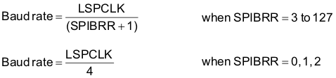
    Baud rate: 125 different programmable rates.

    GUID-5B9E5347-D9EC-4FE9-946C-9A5D76753A23-low.gif
  • Data word length: 1 to 16 data bits
  • Four clocking schemes (controlled by clock polarity and clock phase bits) include:
    • Falling edge without phase delay: SPICLK active-high. SPI transmits data on the falling edge of the SPICLK signal and receives data on the rising edge of the SPICLK signal.
    • Falling edge with phase delay: SPICLK active-high. SPI transmits data one half-cycle ahead of the falling edge of the SPICLK signal and receives data on the falling edge of the SPICLK signal.
    • Rising edge without phase delay: SPICLK inactive-low. SPI transmits data on the rising edge of the SPICLK signal and receives data on the falling edge of the SPICLK signal.
    • Rising edge with phase delay: SPICLK inactive-low. SPI transmits data one half-cycle ahead of the rising edge of the SPICLK signal and receives data on the rising edge of the SPICLK signal.
  • Simultaneous receive and transmit operation (transmit function can be disabled in software)
  • Transmitter and receiver operations are accomplished through either interrupt-driven or polled algorithms.
  • Nine SPI module control registers: Located in control register frame beginning at address 7040h.
    Note:

    All registers in this module are 16-bit registers that are connected to Peripheral Frame 2. When a register is accessed, the register data is in the lower byte (7–0), and the upper byte (15–8) is read as zeros. Writing to the upper byte has no effect.

Enhanced feature:

  • 4-level transmit/receive FIFO
  • Delayed transmit control
  • Bi-directional 3-wire SPI mode support
  • Audio data receive support through SPISTE inversion

Figure 8-28 is a block diagram of the SPI in slave mode.

GUID-F802AE85-ACDA-4C7D-B40B-15F071D3373A-low.gif
SPISTE is driven low by the master for a slave device.
Figure 8-28 SPI Module Block Diagram (Slave Mode)