SCDS408C February 2019 – December 2023 TMUX1111 , TMUX1112 , TMUX1113
PRODUCTION DATA
- 1
- 1 Features
- 2 Applications
- 3 Description
- 4 Device Comparison Table
- 5 Pin Configuration and Functions
-
6 Specifications
- 6.1 Absolute Maximum Ratings
- 6.2 ESD Ratings
- 6.3 Recommended Operating Conditions
- 6.4 Thermal Information
- 6.5 Electrical Characteristics (VDD = 5V ±10 %)
- 6.6 Electrical Characteristics (VDD = 3.3V ±10 %)
- 6.7 Electrical Characteristics (VDD = 1.8V ±10 %)
- 6.8 Electrical Characteristics (VDD = 1.2V ±10 %)
- 6.9 Typical Characteristics
- 7 Parameter Measurement Information
- 8 Detailed Description
- 9 Application and Implementation
- 10Device and Documentation Support
- 11Revision History
- 12Mechanical, Packaging, and Orderable Information
Package Options
Refer to the PDF data sheet for device specific package drawings
Mechanical Data (Package|Pins)
- PW|16
- RSV|16
Thermal pad, mechanical data (Package|Pins)
Orderable Information
3 Description
The TMUX1111, TMUX1112, and TMUX1113 are precision complementary metal-oxide semiconductor (CMOS) devices that have four independently selectable 1:1, single-pole, single-throw (SPST) switches. Wide operating supply of 1.08V to 5.5V allows for use in a broad array of applications from medical equipment to industrial systems. The device supports bidirectional analog and digital signals on the source (Sx) and drain (Dx) pins ranging from GND to VDD.
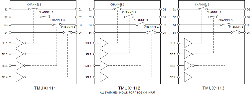
The switches of the TMUX1111 are turned on with Logic 0 on the appropriate logic control inputs, while Logic 1 is required to turn on switches in the TMUX1112. The four channels of the TMUX1113 are split with two switches supporting Logic 0, while the other two switches support Logic 1. The TMUX1113 exhibits break-before-make switching, allowing the device to be used in cross-point switching applications.
The TMUX111x devices are part of the precision switches and multiplexers family. These devices have very low on and off leakage currents and low charge injection, allowing them to be used in high precision measurement applications. A low supply current of 8 nA and small package options enable use in portable applications.
| PART NUMBER(1) | CONTROL LOGIC(1) | PACKAGE(2) |
|---|---|---|
| TMUX1111 | Active Low | PW (TSSOP, 16) RSV (UQFN, 16) |
TMUX1112 | Active High | |
TMUX1113 | Mixed |
 TMUX111x Block Diagrams