SCDS414F december 2019 – july 2023 TMUX1308-Q1 , TMUX1309-Q1
PRODUCTION DATA
- 1
- 1 Features
- 2 Applications
- 3 Description
- 4 Revision History
- 5 Device Comparison Table
- 6 Pin Configuration and Functions
-
7 Specifications
- 7.1 Absolute Maximum Ratings
- 7.2 ESD Ratings
- 7.3 Recommended Operating Conditions
- 7.4 Thermal Information: TMUX1308-Q1
- 7.5 Thermal Information: TMUX1309-Q1
- 7.6 Electrical Characteristics
- 7.7 Logic and Dynamic Characteristics
- 7.8 Timing Characteristics
- 7.9 Injection Current Coupling
- 7.10 Typical Characteristics
- 8 Parameter Measurement Information
-
9 Detailed Description
- 9.1 Overview
- 9.2 Functional Block Diagram
- 9.3
Feature Description
- 9.3.1 Bidirectional Operation
- 9.3.2 Rail-to-Rail Operation
- 9.3.3 1.8 V Logic Compatible Inputs
- 9.3.4 Fail-Safe Logic
- 9.3.5
Injection Current Control
- 9.3.5.1 TMUX13xx-Q1 is Powered, Channel is Unselected, and the Input Signal is Greater Than VDD (VDD = 5 V, VINPUT = 5.5 V)
- 9.3.5.2 TMUX13xx-Q1 is Powered, Channel is Selected, and the Input Signal is Greater Than VDD (VDD = 5 V, VINPUT = 5.5 V)
- 9.3.5.3 TMUX13xx-Q1 is Unpowered and the Input Signal has a Voltage Present (VDD = 0 V, VINPUT = 3 V)
- 9.4 Device Functional Modes
- 9.5 Truth Tables
- 10Application and Implementation
- 11Device and Documentation Support
- 12Mechanical, Packaging, and Orderable Information
Package Options
Mechanical Data (Package|Pins)
Thermal pad, mechanical data (Package|Pins)
- BQB|16
Orderable Information
10.2 Typical Application
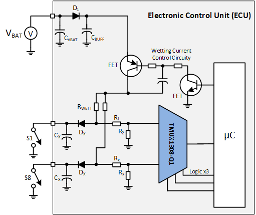
One useful application that takes advantage of the TMUX13xx-Q1 features is multiplexing various physical switches in a body control module (BCM) or electronic control unit (ECU). Automotive BCMs are complex systems designed to manage numerous functions such as lighting, door locks, windows, wipers, turn signals, and many more inputs. The BCM monitors these physical switches and controls power to various loads within the vehicle. A CMOS multiplexer can be used to multiplex the inputs and minimize the number of GPIO or ADC inputs needed by an onboard MCU. Figure 10-1 shows a typical BCM system using the TMUX1308-Q1 to multiplex system inputs.
 Figure 10-1 Multiplexing BCM Inputs