SCDS367E august 2017 – june 2023 TMUX136
PRODUCTION DATA
- 1
- 1 Features
- 2 Applications
- 3 Description
- 4 Revision History
- 5 Pin Configuration and Functions
- 6 Specifications
- 7 Parameter Measurement Information
- 8 Detailed Description
- 9 Application and Implementation
- 10Device and Documentation Support
- 11Mechanical, Packaging, and Orderable Information
Package Options
Refer to the PDF data sheet for device specific package drawings
Mechanical Data (Package|Pins)
- RSE|10
Thermal pad, mechanical data (Package|Pins)
Orderable Information
3 Description
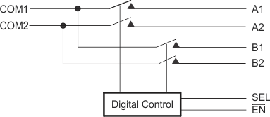
The TMUX136 device is a high performance, 6-GHz, 2-channel, 2:1 switch that will support both differential and single ended signals. The device has a wide VCC range of 2.3 V to 4.8 V and supports a power-off protection feature forcing all I/O pins to be in high-impedance mode when power is not present on the VCC pin. The select pins of TMUX136 are compatible with 1.8-V control voltage, allowing them to be directly interfaced with the General-Purpose I/O (GPIO) from low voltage processors. The flow-through pinout, where inputs and outputs are on opposite sides of the device, simplifies layout routing . This, along with the low on-resistance and low on-capacitance of the device, make the TMUX136 an optimal device for supporting switching a wide range of analog signals and digital communication protocol standards, including high-speed standards such as I3C.
The TMUX136 comes in a small 10-pin UQFN package with only 1.5 mm × 2 mm in size, which makes it useful when PCB area is limited.
 Simplified Schematic
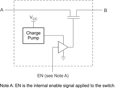
 Functional Block
Diagram