SCDS428A March 2020 – March 2021 TMUX4157N
PRODUCTION DATA
- 1 Features
- 2 Applications
- 3 Description
- 4 Revision History
- 5 Pin Configuration and Functions
- 6 Specifications
- 7 Parameter Measurement Information
- 8 Detailed Description
- 9 Application and Implementation
- 10Power Supply Recommendations
- 11Layout
- 12Device and Documentation Support
- 13Mechanical, Packaging, and Orderable Information
Package Options
Mechanical Data (Package|Pins)
- DCK|6
Thermal pad, mechanical data (Package|Pins)
Orderable Information
3 Description
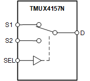
The TMUX4157N is a general purpose 2:1, single-pole double-throw (SPDT), switch that supports a negative supply rail only. The supply voltage can range from -4 V to -12 V and the device supports bidirectional analog and digital signals on the source (Sx) and drain (D) pins ranging from GND to VSS. The state of the select pin (SEL) controls which of the two sources pins are connected to the drain pin.
While TMUX4157N supports negative voltages on the supply pin and signal path, the logic input pin is controlled with a positive voltage to allow interfacing with typical control logic circuitry such as a GPIO signal. The logic input pin has 1.8 V logic compatible thresholds and can operate as high as 5.5 for added system flexibility. Fail-Safe Logic circuitry allows voltages on the control pins to be applied before the supply pin, protecting the device from potential damage.
Fast transition times and high continuous current through the switch make the TMUX4157N well suited for applications where the system needs to quickly switch between two different voltage inputs.
| PART NUMBER(1) | PACKAGE | BODY SIZE (NOM) |
|---|---|---|
| TMUX4157N | SC70 (6) | 2.00 mm × 1.25 mm |
 TMUX4157N Block Diagram
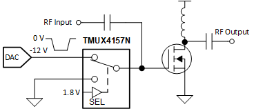
 Application Example