SCDS398A December 2018 – July 2022 TMUX6121 , TMUX6122 , TMUX6123
PRODUCTION DATA
- 1 Features
- 2 Applications
- 3 Description
- 4 Revision History
- 5 Pin Configuration and Functions
-
6 Specifications
- 6.1 Absolute Maximum Ratings
- 6.2 ESD Ratings
- 6.3 Thermal Information
- 6.4 Recommended Operating Conditions
- 6.5 Electrical Characteristics (Dual Supplies: ±15 V)
- 6.6 Switching Characteristics (Dual Supplies: ±15 V)
- 6.7 Electrical Characteristics (Single Supply: 12 V)
- 6.8 Switching Characteristics (Single Supply: 12 V)
- Typical Characteristics
- 7 Parameter Measurement Information
- 8 Detailed Description
- 9 Application and Implementation
- 10Power Supply Recommendations
- 11Layout
- 12Device and Documentation Support
- 13Mechanical, Packaging, and Orderable Information
Package Options
Mechanical Data (Package|Pins)
- DGS|10
Thermal pad, mechanical data (Package|Pins)
Orderable Information
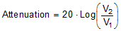
8.1.9 Bandwidth
Bandwidth is defined as the range of frequencies that are attenuated by < 3 dB when the input is applied to the source pin (Sx) of an on-channel, and the output is measured at the drain pin (D) of the TMUX6121, TMUX6122, and TMUX6123. Figure 8-9 shows the setup used to measure bandwidth of the switch. Use Equation 4 to compute the attenuation.
 Figure 8-9 Bandwidth Measurement Setup
Equation 4.