SCDS442C July 2020 – July 2024 TMUX6234
PRODUCTION DATA
- 1
- 1 Features
- 2 Applications
- 3 Description
- 4 Pin Configuration and Functions
-
5 Specifications
- 5.1 Absolute Maximum Ratings
- 5.2 ESD Ratings
- 5.3 Thermal Information
- 5.4 Recommended Operating Conditions
- 5.5 Source or Drain Continuous Current
- 5.6 36 V Single Supply: Electrical Characteristics
- 5.7 36 V Single Supply: Switching Characteristics
- 5.8 ±15 V Dual Supply: Electrical Characteristics
- 5.9 ±15 V Dual Supply: Switching Characteristics
- 5.10 12 V Single Supply: Electrical Characteristics
- 5.11 12 V Single Supply: Switching Characteristics
- 5.12 ±5 V Dual Supply: Electrical Characteristics
- 5.13 ±5 V Dual Supply: Switching Characteristics
- 5.14 Typical Characteristics
-
6 Parameter Measurement Information
- 6.1 On-Resistance
- 6.2 Off-Leakage Current
- 6.3 On-Leakage Current
- 6.4 Transition Time
- 6.5 tON(EN) and tOFF(EN)
- 6.6 Break-Before-Make
- 6.7 tON (VDD) Time
- 6.8 Propagation Delay
- 6.9 Charge Injection
- 6.10 Off Isolation
- 6.11 Crosstalk
- 6.12 Bandwidth
- 6.13 THD + Noise
- 6.14 Power Supply Rejection Ratio (PSRR)
- 7 Detailed Description
- 8 Application and Implementation
- 9 Device and Documentation Support
- 10Revision History
- 11Mechanical, Packaging, and Orderable Information
Package Options
Mechanical Data (Package|Pins)
Thermal pad, mechanical data (Package|Pins)
Orderable Information
8.2 Typical Application
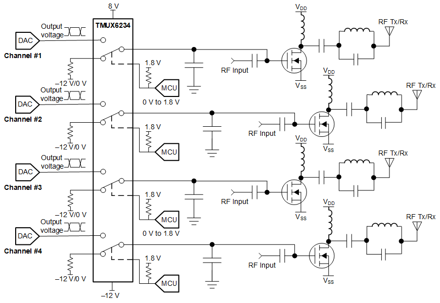
One application of the TMUX6234 is for input control of a power amplifier gate driver. Utilizing a switch allows a system to control when the DAC is connected to the power amplifier, and can stop biasing the power amplifier by switching the gate voltage. The wide dual supply range of ±4.5 V to ±18 V allows the switch to work with GaN power amplifiers and the wide single supply range 4.5 V to 36 V works well with LDMOS power amplifiers.
Figure 8-1 shows the TMUX6234 configured for control of a multi-channel power amplifier application.
 Figure 8-1 Power Amplifier Gate Driver