SLOS717B August 2011 – December 2014 TPA2025D1
PRODUCTION DATA.
- 1 Features
- 2 Applications
- 3 Description
- 4 Revision History
- 5 Device Comparison Table
- 6 Pin Configuration and Functions
- 7 Specifications
- 8 Parameter Measurement Information
- 9 Detailed Description
- 10Application and Implementation
- 11Power Supply Recommendations
- 12Layout
- 13Device and Documentation Support
- 14Mechanical, Packaging, and Orderable Information
Package Options
Mechanical Data (Package|Pins)
- YZG|12
Thermal pad, mechanical data (Package|Pins)
Orderable Information
10 Application and Implementation
NOTE
Information in the following applications sections is not part of the TI component specification, and TI does not warrant its accuracy or completeness. TI’s customers are responsible for determining suitability of components for their purposes. Customers should validate and test their design implementation to confirm system functionality.
10.1 Application Information
The TPA2025D1 is a Class D amplifier with integrated automatic gain control and boost converter. This device is capable of drive up to 1.9W to 8-Ω Speaker (1% THD+N). TPA2025D1 starts operating when setting EN pin to HIGH level. The device enters in shutdown mode when asserting EN to LOW level. AGC pin connection sets the threshold where the device will start reducing the output amplitude. The selectable threshold voltages are specified in the Operating Characteristics section. In order to measure the TPA2025D1 output with an analyzer, a 30KHz Low pass filter should be implemented.
10.2 Typical Application
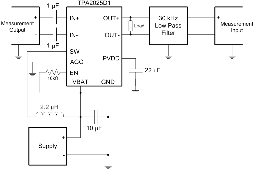
10.2.1 Design Requirements
For this design example, use the parameters listed in Table 1.
Table 1. Design Parameters
| PARAMETER | VALUE |
|---|---|
| Supply voltage range | 2.5 V - 5.2 V |
| Input voltage range | 0 V - 5 V |
| Peak output voltage | 5.45 V |
| Max output current | 1.8 A |
10.2.2 Detailed Design Procedure
10.2.2.1 Boost Converter Component Section
The critical external components are summarized in the following table:
| PARAMETER | TEST CONDITIONS | MIN | TYP | MAX | UNIT |
|---|---|---|---|---|---|
| Boost converter inductor | At 30% rated DC bias current of the inductor | 1.5 | 2.2 | 4.7 | µH |
| Boost converter input capacitor | 4.7 | 10 | µF | ||
| Boost converter output capacitor | Working capacitance biased at boost output voltage, if 4.7µH inductor is chosen, then minimum capacitance is 10 µF | 4.7 | 22 | µF |
10.2.2.1.1 Inductor Equations
Inductor current rating is determined by the requirements of the load. The inductance is determined by two factors: the minimum value required for stability and the maximum ripple current permitted in the application. Use Equation 1 to determine the required current rating. Equation 1 shows the approximate relationship between the average inductor current, IL, to the load current, load voltage, and input voltage (IPVDD, PVDD, and VBAT, respectively). Insert IPVDD, PVDD, and VBAT into Equation 1 and solve for IL. The inductor must maintain at least 90% of its initial inductance value at this current.
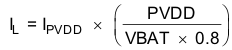
Ripple current, ΔIL, is peak-to-peak variation in inductor current. Smaller ripple current reduces core losses in the inductor and reduces the potential for EMI. Use Equation 2 to determine the value of the inductor, L. Equation 2 shows the relationship between inductance L, VBAT, PVDD, the switching frequency, fBOOST, and ΔIL. Insert the maximum acceptable ripple current into Equation 2 and solve for L.
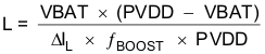
ΔIL is inversely proportional to L. Minimize ΔIL as much as is necessary for a specific application. Increase the inductance to reduce the ripple current. Do not use greater than 4.7 μH, as this prevents the boost converter from responding to fast output current changes properly. If using above 3.3 µH, then use at least 10 µF capacitance on PVDD to ensure boost converter stability.
The typical inductor value range for the TPA2025D1 is 2.2 μH to 3.3 µH. Select an inductor with less than 0.5 Ω dc resistance, DCR. Higher DCR reduces total efficiency due to an increase in voltage drop across the inductor.
Table 2. Sample Inductors
| L (µH) |
SUPPLIER | COMPONENT CODE | SIZE (LxWxH mm) |
DCR TYP (mΩ) |
ISAT MAX (A) |
C RANGE |
|---|---|---|---|---|---|---|
| 2.2 | Toko | 1239AS-H-2R2N=P2 | 2.5 x 2.0 x 1.2 | 96 | 2.3 | 4.7 - 22 µF / 16 V 6.8 - 22 µV / 10 V |
| 2.2 | Coilcraft | XFL4020-222MEC | 4.0 x 4.0 x 2.15 | 22 | 3.5 | |
| 3.3 | Toko | 1239AS-H-3R3N=P2 | 2.5 x 2.0 x 1.2 | 160 | 2.0 | 10 - 22 µF / 10 V |
| 3.3 | Coilcraft | XFL4020-332MEC | 4.0 x 4.0 x 2.15 | 35 | 2.8 |
10.2.2.1.2 Boost Converter Capacitor Selection
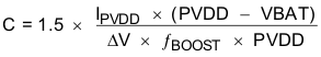
The value of the boost capacitor is determined by the minimum value of working capacitance required for stability and the maximum voltage ripple allowed on PVDD in the application. Working capacitance refers to the available capacitance after derating the capacitor value for DC bias, temperature, and aging. Do not use any component with a working capacitance less than 4.7 µF. This corresponds to a 4.7 μF/16 V capacitor, or a 6.8 μF/10 V capacitor.
Do not use above 22 μF capacitance as it will reduce the boost converter response time to large output current transients.
Equation 3 shows the relationship between the boost capacitance, C, to load current, load voltage, ripple voltage, input voltage, and switching frequency (IPVDD, PVDD, ΔV, VBAT, and fBOOST respectively).
Insert the maximum allowed ripple voltage into Equation 3 and solve for C. The 1.5 multiplier accounts for capacitance loss due to applied dc voltage and temperature for X5R and X7R ceramic capacitors.
10.2.2.1.3 Boost Terms
The following is a list of terms and definitions used in the boost equations.
| C | Minimum boost capacitance required for a given ripple voltage on PVDD. |
| L | Boost inductor |
| fBOOST | Switching frequency of the boost converter. |
| IPVDD | Current pulled by the Class-D amplifier from the boost converter. |
| IL | Average current through the boost inductor. |
| PVDD | Supply voltage for the Class-D amplifier. (Voltage generated by the boost converter output) |
| VBAT | Supply voltage to the IC. |
| ΔIL | Ripple current through the inductor. |
| ΔV | Ripple voltage on PVDD. |
10.2.2.2 Input Capacitors
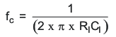
Input audio DC decoupling capacitors are recommended. The input audio DC decoupling capacitors prevents the AGC from changing the gain due to audio DAC output offset. The input capacitors and TPA2025D1 input impedance form a high-pass filter with the corner frequency, fC, determined in Equation 4.
Any mismatch in capacitance between the two inputs will cause a mismatch in the corner frequencies. Severe mismatch may also cause turn-on pop noise. Choose capacitors with a tolerance of ±10% or better.
10.2.2.3 Speaker Load Limitation
Speakers are non-linear loads with varying impedance (magnitude and phase) over the audio frequency. A portion of speaker load current can flow back into the boost converter output via the Class-D output H-bridge high-side device. This is dependent on the speaker's phase change over frequency, and the audio signal amplitude and frequency content. Most portable speakers have limited phase change at the resonant frequency, typically no more than 40 or 50 degrees. To avoid excess flow-back current, use speakers with limited phase change. Otherwise, flow-back current could drive the PVDD voltage above the absolute maximum recommended operational voltage.
Confirm proper operation by connecting the speaker to the TPA2025D1 and driving it at maximum output swing. Observe the PVDD voltage with an oscilloscope. In the unlikely event the PVDD voltage exceeds 6.5 V, add a 6.8 V Zener diode between PVDD and ground to ensure the TPA2025D1 operates properly. The amplifier has thermal overload protection and deactivates if the die temperature exceeds 150°C. It automatically reactivates once die temperature returns below 150°C. Built-in output over-current protection deactivates the amplifier if the speaker load becomes short-circuited. The amplifier automatically restarts 1.6 seconds after the over-current event. Although the TPA2025D1 Class-D output can withstand a short between OUT+ and OUT-, do not connect either output directly to GND, VDD, or VBAT as this could damage the device.
10.2.3 Application Curve
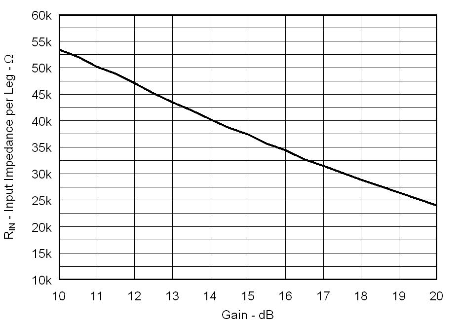 Figure 26. Input Impedance vs Gain
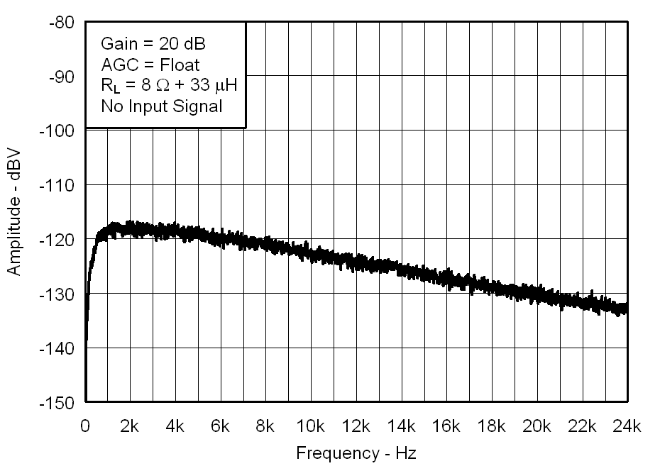 Figure 28. A-Weighted Noise vs Frequency
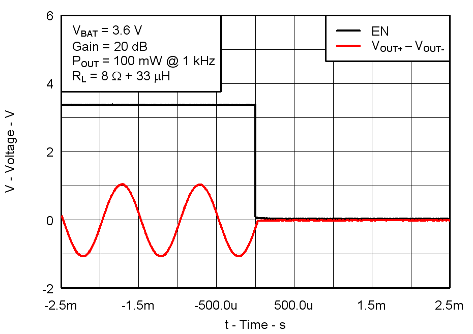 Figure 30. Shutdown Timing
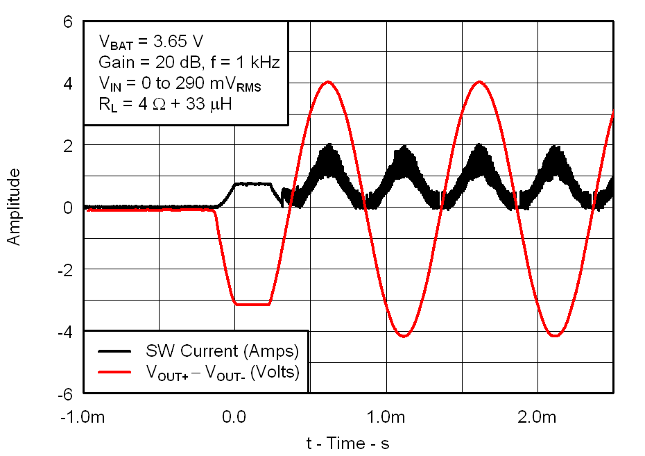 Figure 27. Boost Startup Current vs Time
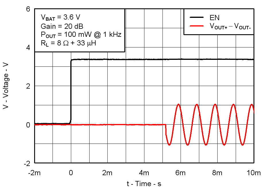 Figure 29. Startup Timing
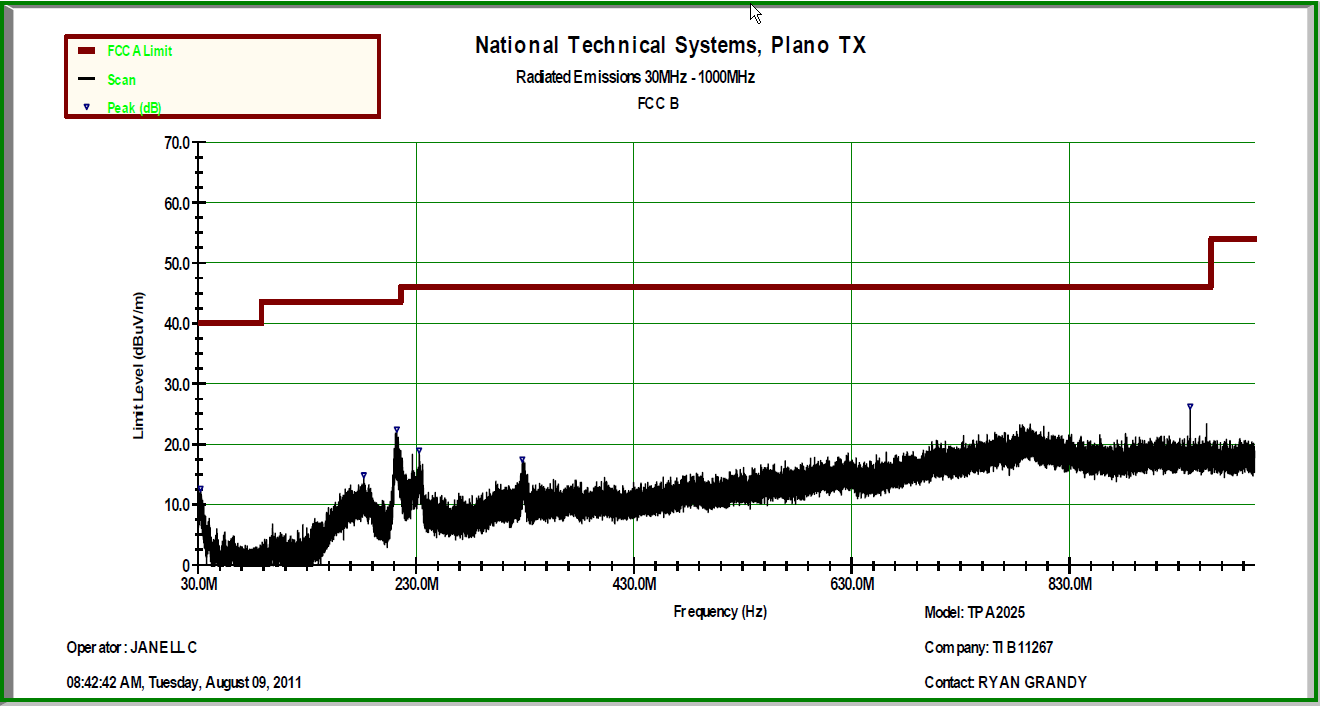 Figure 31. EMC Performance Po = 750 mW with 2 Inch Speaker Cable