SLOS717B August 2011 – December 2014 TPA2025D1
PRODUCTION DATA.
- 1 Features
- 2 Applications
- 3 Description
- 4 Revision History
- 5 Device Comparison Table
- 6 Pin Configuration and Functions
- 7 Specifications
- 8 Parameter Measurement Information
- 9 Detailed Description
- 10Application and Implementation
- 11Power Supply Recommendations
- 12Layout
- 13Device and Documentation Support
- 14Mechanical, Packaging, and Orderable Information
Package Options
Mechanical Data (Package|Pins)
- YZG|12
Thermal pad, mechanical data (Package|Pins)
Orderable Information
7 Specifications
7.1 Absolute Maximum Ratings
Over operating free–air temperature range, TA= 25°C (unless otherwise noted)(1)| MIN | MAX | UNIT | ||
|---|---|---|---|---|
| Supply voltage | VBAT | –0.3 | 6 | V |
| Input Voltage, VI | IN+, IN– | –0.3 | VBAT + 0.3 | V |
| Output continuous total power dissipation | See Thermal Information | |||
| Operating free-air temperature range, TA | –40 | 85 | °C | |
| Operating junction temperature range, TJ | –40 | 150 | °C | |
| Minimum load resistance | 3.2 | Ω | ||
| Maximum input voltage swing | EN = 0 V | 2 | VRMS | |
| Storage temperature range, Tstg | –65 | 150 | °C | |
(1) Stresses beyond those listed under Absolute Maximum Ratings may cause permanent damage to the device. These are stress ratings only, and functional operation of the device at these or any other conditions beyond those indicated under Recommended Operating Conditions is not implied. Exposure to absolute–maximum–rated conditions for extended periods may affect device reliability.
7.2 ESD Ratings
| VALUE | UNIT | |||
|---|---|---|---|---|
| V(ESD) | Electrostatic discharge | Human-body model (HBM), per ANSI/ESDA/JEDEC JS-001(1) | ±2000 | V |
| Charged-device model (CDM), per JEDEC specification JESD22-C101(2) | ±500 | |||
| Machine model (MM) | ±100 | |||
(1) JEDEC document JEP155 states that 500-V HBM allows safe manufacturing with a standard ESD control process.
(2) JEDEC document JEP157 states that 250-V CDM allows safe manufacturing with a standard ESD control process.
7.3 Recommended Operating Conditions
| MIN | MAX | UNIT | ||
|---|---|---|---|---|
| Supply voltage, VBAT | 2.5 | 5.2 | V | |
| VIH | High–level input voltage, EN | 1.3 | V | |
| VIL | Low–level input voltage, EN | 0.6 | V | |
| TA | Operating free-air temperature | –40 | 85 | °C |
| TJ | Operating junction temperature | –40 | 150 | °C |
7.4 Thermal Information
| THERMAL METRIC(1) | TPA2025D1 | UNITS | |
|---|---|---|---|
| YZG | |||
| 12 PINS | |||
| RθJA | Junction-to-ambient thermal resistance | 97.3 | °C/W |
| RθJC(top) | Junction-to-case(top) thermal resistance | 36.7 | |
| RθJB | Junction-to-board thermal resistance | 55.9 | |
| ψJT | Junction-to-top characterization parameter | 13.9 | |
| ψJB | Junction-to-board characterization parameter | 49.5 | |
(1) For more information about traditional and new thermal metrics, see the IC Package Thermal Metrics application report, SPRA953.
7.5 Electrical Characteristics
VBAT = 3.6 V, TA = 25°C, RL = 8 Ω + 33 μH (unless otherwise noted)7.6 Operating Characteristics
VBAT= 3.6 V, EN = VBAT, AGC = GND, TA = 25°C, RL = 8 Ω + 33 μH (unless otherwise noted)| PARAMETER | TEST CONDITIONS | MIN | TYP | MAX | UNIT | |
|---|---|---|---|---|---|---|
| BOOST CONVERTER | ||||||
| PVDD | Boost converter output voltage range | IBOOST = 0 mA | 5.4 | 5.75 | 6.4 | V |
| IBOOST = 700 mA | 5.6 | V | ||||
| IL | Boost converter input current limit | Power supply current | 1800 | mA | ||
| Boost converter start-up current limit | Boost converter starts up from full shutdown | 600 | ||||
| Boost converter wakes up from auto-pass through mode | 1000 | |||||
| fBOOST | Boost converter frequency | 1.2 | MHz | |||
| CLASS-D AMPLIFIER | ||||||
| PO | Output power | THD = 1%, VBAT = 2.5 V, f = 1 kHz | 1440 | mW | ||
| THD = 1%, VBAT = 3.0 V, f = 1 kHz | 1750 | |||||
| THD = 1%, VBAT = 3.6 V, f = 1 kHz | 1900 | |||||
| THD = 1%, VBAT = 2.5 V, f = 1 kHz, RL = 4 Ω + 33 µH |
1460 | |||||
| THD = 1%, VBAT = 3.0 V, f = 1 kHz, RL = 4 Ω + 33 µH |
1800 | |||||
| THD = 1%, VBAT = 3.6 V, f = 1 kHz, RL = 4 Ω + 33 µH |
2280 | |||||
| VO | Peak output voltage | THD = 1%, VBAT = 3.6 V, f = 1 kHz, 6 dB crest factor sine burst, no clipping | 5.45 | V | ||
| AV | Voltage gain | 19.5 | 20 | 20.5 | dB | |
| |VOOS | | Output offset voltage | 2 | 10 | mV | ||
| Short-circuit protection threshold current | 2 | A | ||||
| RIN | Input impedance (per input pin) | AV = 20 dB | 24 | kΩ | ||
| Input impedance in shutdown (per input pin) | EN = 0 V | 1300 | ||||
| ZO | Output impedance in shutdown | 2 | kΩ | |||
| Boost converter auto-pass through threshold | Class-D output voltage threshold when boost converter automatically turns on | 2 | VPK | |||
| fCLASS-D | Class-D switching frequency | 275 | 300 | 325 | kHz | |
| η | Class-D and boost combined efficiency | PO = 1 W, VBAT = 3.6 V | 82% | |||
| EN | Noise output voltage | A-weighted | 49 | μVRMS | ||
| Unweighted | 65 | |||||
| SNR | Signal-to-noise ratio | 1.7 W, RL = 8 Ω + 33 µH. A-weighted | 97 | dB | ||
| 1.7 W, RL = 8 Ω + 33 µH. Unweighted | 95 | |||||
| 2 W, RL = 4 Ω + 33 µH. A-weighted | 95 | |||||
| 2 W, RL = 4 Ω + 33 µH. Unweighted | 93 | |||||
| THD+N | Total harmonic distortion plus noise(1) | PO = 100 mW, f = 1 kHz | 0.06% | |||
| PO = 500 mW, f = 1 kHz | 0.07% | |||||
| PO = 1.7 W, f = 1 kHz, RL = 8 Ω + 33 µH | 0.07% | |||||
| PO = 2 W, f = 1 kHz, RL = 4 Ω + 33 µH | 0.15% | |||||
| THD+N added to other audio signal connected at amplifier input during shutdown | 0.02% | |||||
| AC PSRR | AC-Power supply ripple rejection (output referred) | 200 mVPP square ripple, VBAT = 3.8 V, f = 217 Hz | 62.5 | dB | ||
| 200 mVPP square ripple, VBAT = 3.8 V, f = 1 kHz | 62.5 | |||||
| AC CMRR | AC-Common mode rejection ratio (output referred) | 200 mVPP square ripple, VBAT = 3.8 V, f = 217 Hz | 71 | dB | ||
| 200 mVPP square ripple, VBAT = 3.8 V, f = 1 kHz | 71 | |||||
| AUTOMATIC GAIN CONTROL | ||||||
| AGC maximum attenuation | 10 | dB | ||||
| AGC attenuation resolution | 0.5 | dB | ||||
| AGC attack time (gain decrease) | 20 | µs/dB | ||||
| AGC release time (gain increase) | 1.6 | s/dB | ||||
| Gain vs VBAT slope | VBAT < inflection point | 7.5 | dB/V | |||
| AGC inflection point (Note: AGC pin voltage is read only at device power-up. A device power cycle is required to change AGC inflection points.) |
AGC = Float | 3.25 | V | |||
| AGC = GND | 3.55 | |||||
| AGC = VBAT | 3.75 | |||||
(1) A-weighted
7.7 Typical Characteristics
VBAT = 3.6 V, CI = 1 µF, CBOOST = 22 µF, LBOOST = 2.2 µH, EN = VBAT, and Load = 8 Ω + 33 µH, no ferrite bead unless otherwise specified.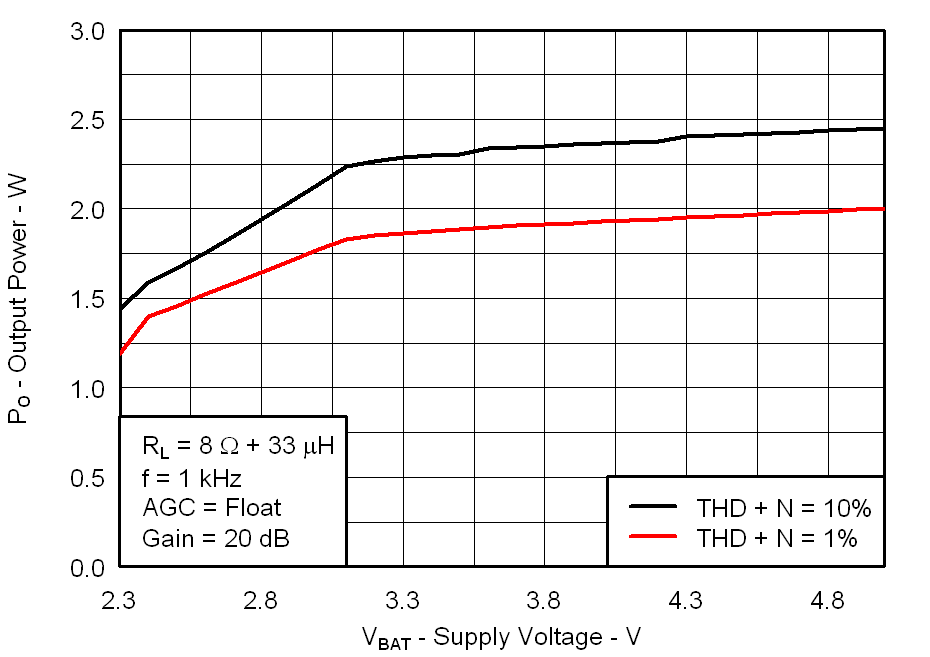 Figure 1. Output Power vs Supply Voltage
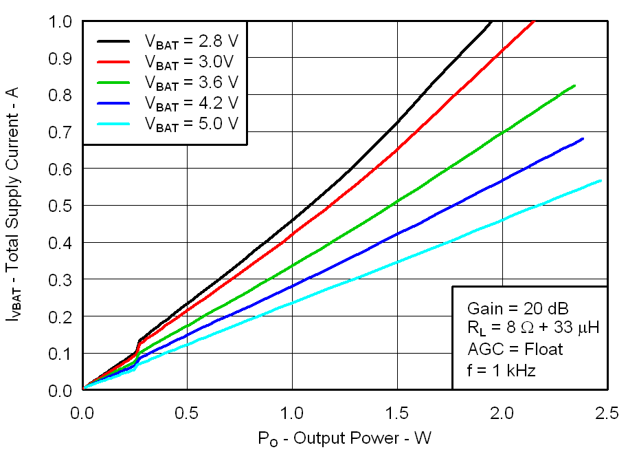 Figure 3. Total Supply Current vs Output Power
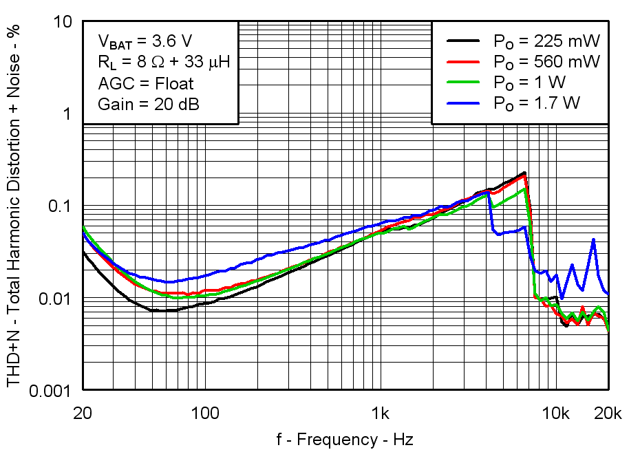 Figure 5. Total Harmonic Distortion + Noise vs Frequency
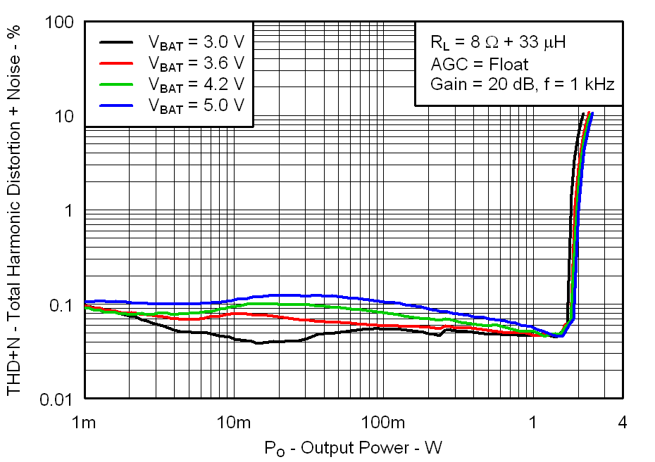 Figure 7. Total Harmonic Distortion + Noise vs Output Power
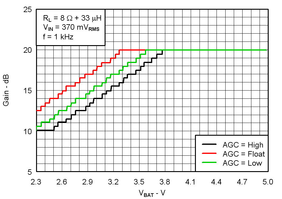 Figure 9. Gain vs Supply Voltage
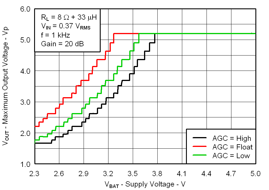 Figure 11. Maximum Peak Output Voltage vs Supply Voltage
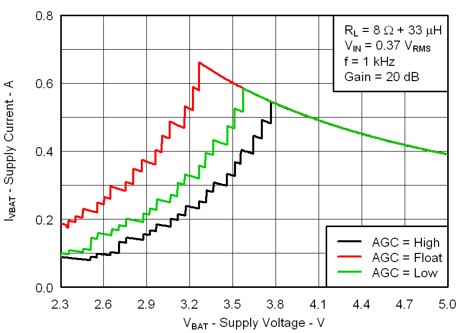 Figure 13. Supply Current vs Supply Voltage
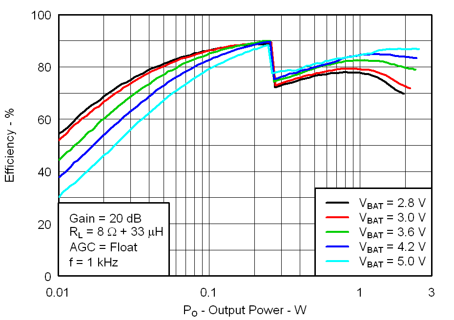 Figure 15. Total Efficiency vs Output Power
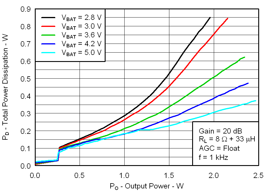 Figure 17. Total Power Dissipation vs Output Power
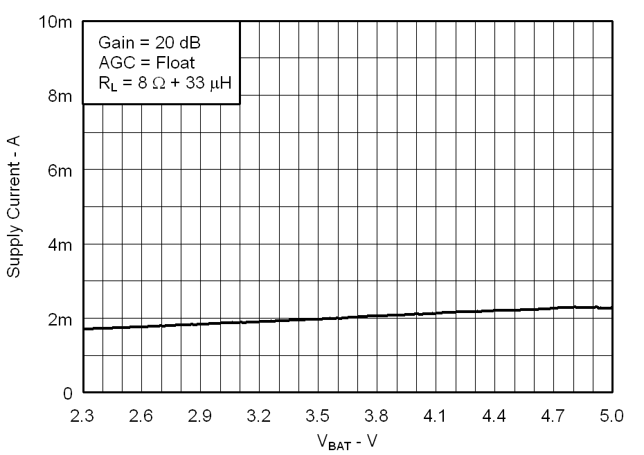 Figure 19. Quiescent Supply Current vs Supply Voltage
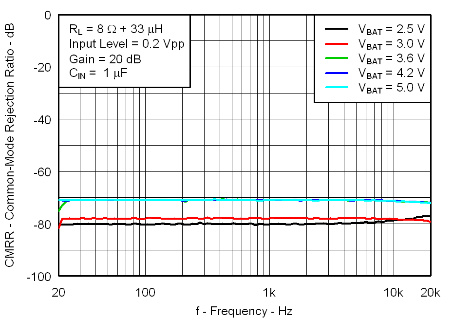 Figure 21. Common Mode Rejection Ratio vs Frequency
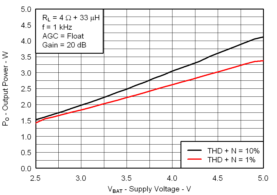 Figure 2. Output Power vs Supply Voltage
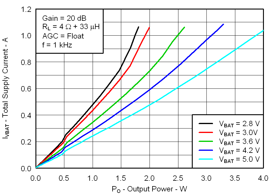 Figure 4. Total Supply Current vs Output Power
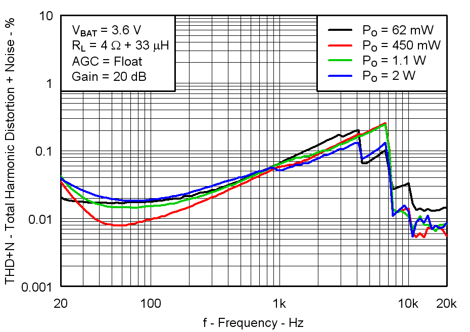 Figure 6. Total Harmonic Distortion + Noise vs Frequency
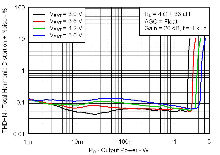 Figure 8. Total Harmonic Distortion + Noise vs Output Power
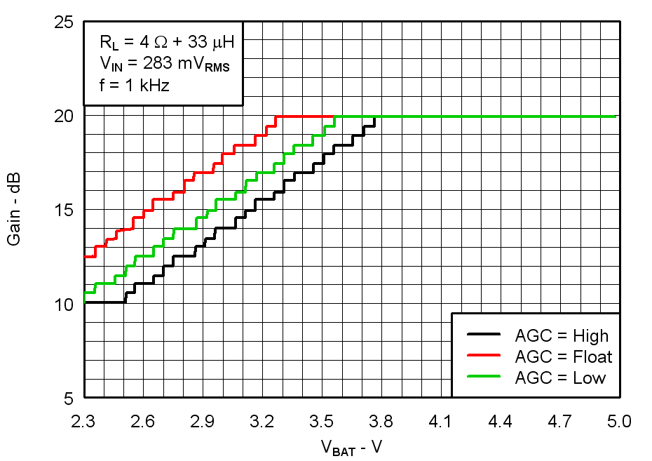 Figure 10. Gain vs Supply Voltage
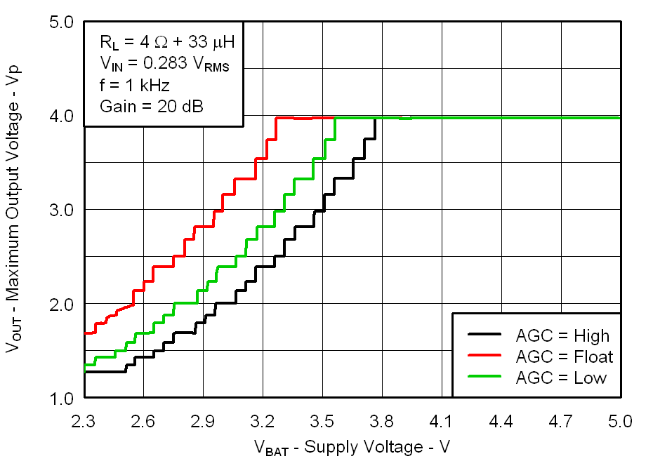 Figure 12. Maximum Peak Output Voltage vs Supply Voltage
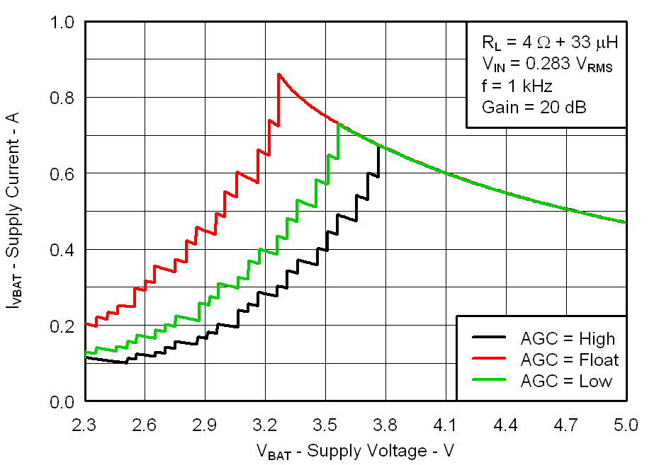 Figure 14. Supply Current vs Supply Voltage
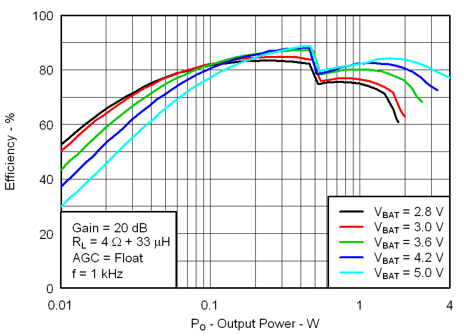 Figure 16. Total Efficiency vs Output Power
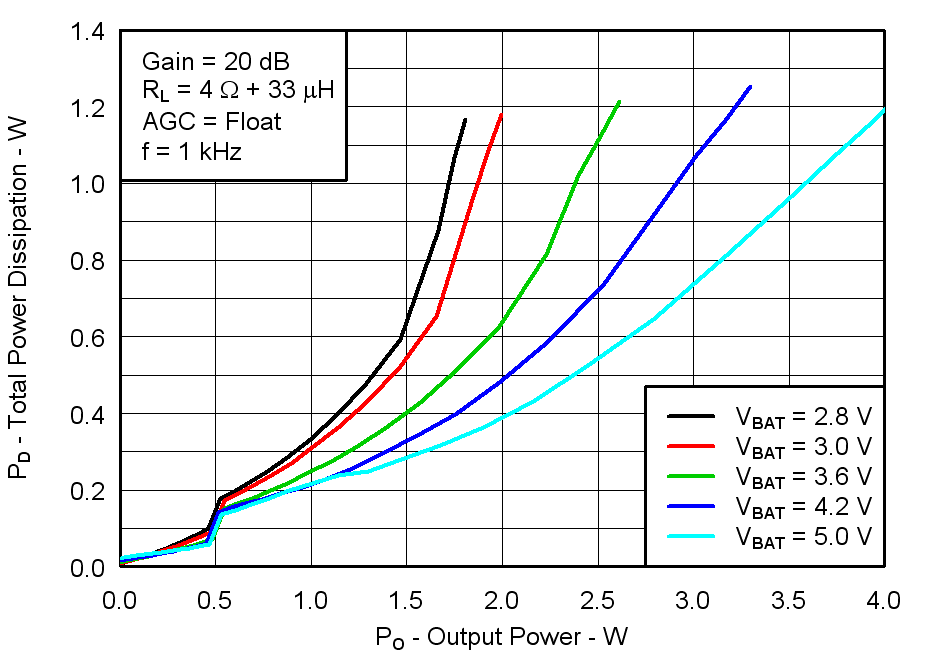 Figure 18. Total Power Dissipation vs Output Power
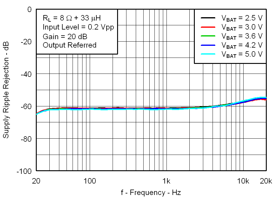 Figure 20. Supply Ripple Rejection vs Frequency