SLOS717B August 2011 – December 2014 TPA2025D1
PRODUCTION DATA.
- 1 Features
- 2 Applications
- 3 Description
- 4 Revision History
- 5 Device Comparison Table
- 6 Pin Configuration and Functions
- 7 Specifications
- 8 Parameter Measurement Information
- 9 Detailed Description
- 10Application and Implementation
- 11Power Supply Recommendations
- 12Layout
- 13Device and Documentation Support
- 14Mechanical, Packaging, and Orderable Information
Package Options
Mechanical Data (Package|Pins)
- YZG|12
Thermal pad, mechanical data (Package|Pins)
Orderable Information
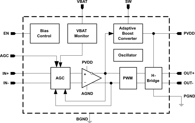
9 Detailed Description
9.1 Overview
The TPA2025D1 is a constant output, high efficiency Class-D audio amplifier with battery tracking AGC technology and an integrated Class-G boost converter. This features give the device a great performance and enhances efficiency at low output power. The TPA2025D1 can drive up to 1.9 W into an 8-Ω speaker (1% THD+N).
The built-in boost converter operates from a battery supply voltage and generates a higher output voltage PVDD at 5.75 V that drives the supply voltage of the Class-D amplifier. This provides a louder audio output than a stand-alone amplifier directly connected to the battery.
The battery tracking AGC adjusts the Class-D gain to limit battery current at lower battery voltage. This lets the device to extend the battery life while playing audio, typically with 85% efficiency. When the battery voltage is below a certain threshold voltage, The TPA2025D1 lowers the audio loudness. The threshold is selectable with an external pin.
The TPA2025D1 has an integrated low-pass filter to improve the RF rejection and reduce DAC out-of-band noise, increasing the signal-to-noise ratio (SNR). The features included in this device allow it to be used in a wide range of portable applications.
9.2 Functional Block Diagram
9.3 Feature Description
9.3.1 Battery Tracking Automatic Gain Control (AGC)
TPA2025D1 monitors the battery voltage and automatically reduces the gain when the battery voltage is below a certain threshold voltage, which is defined as inflection point. Although battery tracking AGC lowers the audio loudness, it prevents high battery current at end-of-charge battery voltage. The inflection point is selectable at AGC pin. When the amplifier is turned on, the gain is set according to battery voltage and selected inflection point.
Figure 22 shows the plot of gain as a function of battery supply voltage. The default slope is 7.5 dB/V. When battery voltage drops below inflection point by 1 V, AGC reduces the gain by 7.5 dB. The TPA2025D1 can only operate at one slope.
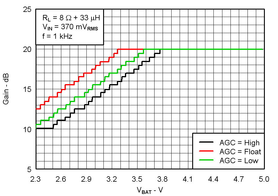 Figure 22. Gain vs Battery voltage
9.3.2 Boost Converter Auto Pass Through (APT)
The TPA2025D1 consists of an adaptive boost converter and a Class-D amplifier. The boost converter operates from the supply voltage, VBAT, and generates a higher output voltage PVDD at 5.75 V. PVDD drives the supply voltage of the Class-D amplifier. This improves loudness over non-boosted solutions. The boost converter has a “Pass Through” mode in which it turns off automatically and PVDD is directly connected to VBAT through an internal bypass switch.
The boost converter is adaptive and operates between pass through mode and boost mode depending on the output audio signal amplitude. When the audio output amplitude exceeds the “auto pass through” (APT) threshold, the boost converter is activated automatically and goes to boost mode. The transition time from normal mode to boost mode is less than 3 ms. TPA2025D1’s APT threshold is fixed at 2 Vpk. When the audio output signal is below APT threshold, the boost converter is deactivated and goes to pass through mode. The adaptive boost converter maximizes system efficiency in lower audio output level.
The battery AGC is independent of APT threshold. The AGC operates in both boost-active and APT modes.
Figure 23 shows how the adaptive boost converter behaves with a typical audio signal.
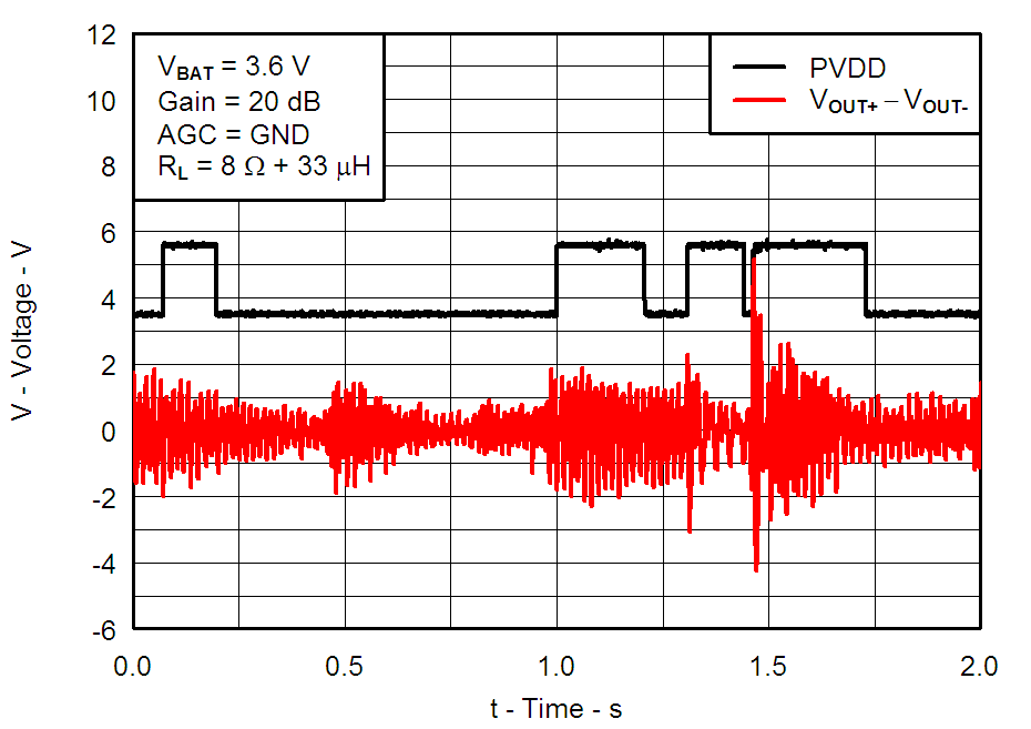 Figure 23. Adaptive Boost Converter with Typical Music Playback
9.3.3 Short Circuit Auto-Recovery
When a short circuit event happens, the TPA2025D1 goes to low duty cycle mode and tries to reactivate itself every 1.6 seconds. This auto-recovery continues until the short circuit event stops. This feature protects the device without affecting its long term reliability.
9.3.4 Thermal Protection
It is important to operate the TPA2025D1 at temperatures lower than its maximum operating temperature. The maximum ambient temperature depends on the heat-sinking ability of the PCB system. Given θJA of 97.3°C/W, the maximum allowable junction temperature of 150°C, and the internal dissipation of 0.5 W for 1.9 W, 8 Ω load, 3.6 V supply, the maximum ambient temperature is calculated as:
TA,MAX = TJ,MAX – θJA PD = 150°C – (97.3°C/W × 0.5W) = 101.4°C
The calculated maximum ambient temperature is 101.4°C at maximum power dissipation at 3.6 V supply and 8 Ω load. The TPA2025D1 is designed with thermal protection that turns the device off when the junction temperature surpasses 150°C to prevent damage to the IC.
9.3.5 Operation with DACS and Codecs
Large noise voltages can be present at the output of ΔΣ DACs and CODECs, just above the audio frequency (e.g: 80 kHz with a 300 mVP-P). This out-of-band noise is due to the noise shaping of the delta-sigma modulator in the DAC. Some Class-D amplifiers have higher output noise when used in combination with these DACs and CODECs. This is because out-of-band noise from the CODEC/DAC mixes with the Class-D switching frequencies in the audio amplifier input stage. The TPA2025D1 has a built-in low-pass filter with cutoff frequency at 55 kHz that reduces the out-of-band noise and RF noise, filtering out-of-band frequencies that could degrade in-band noise performance. This built-in filter also prevents AGC errors due to out-of-band noise. The TPA2025D1 AGC calculates gain based on input signal amplitude only. If driving the TPA2025D1 input with 4th-order or higher ΔΣ DACs or CODECs, add an R-C low pass filter at each of the audio inputs (IN+ and IN-) of the TPA2025D1 to ensure best performance. The recommended resistor value is 100 Ω and the capacitor value of 47 nF.
9.4 Device Functional Modes
9.4.1 Operation Below AGC Threshold
When the battery power supply voltage is below a certain threshold voltage, the TPA2025D1 starts reducing the gain automatically. This AGC threshold is selected by external AGC pin at 3.25 V, 3.55 V and 3.75 V for FLOAT, LOW and HIGH levels respectively.
Figure 24 shows the operation of AGC in time domain.
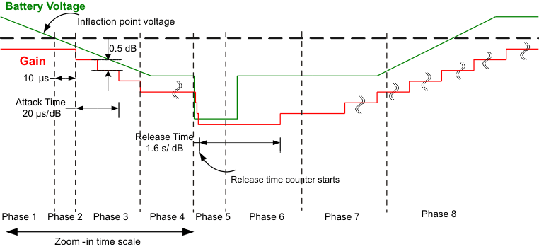 Figure 24. Relationship Between Supply Voltage and Gain in Time Domain
| Phase 1 | Battery discharging normally; supply voltage is above inflection point; audio gain remains at 20 dB. |
| Phase 2 | Battery voltage decreases below inflection point. AGC responds in 10 μs and reduces gain by one step (0.5 dB) |
| Phase 3 | Battery voltage continues to decrease. AGC continues to reduce gain. The rate of gain decrease is defined as attack time. TPA2025D1’s attack time is 20 µs/dB. |
| Phase 4 | Battery voltage is constant. AGC stops reducing gain. |
| Phase 5 | Battery voltage decreases suddenly. AGC reduces gain multiple steps. (time scale from this phase is longer) Release time counter resets every end of attack event. |
| Phase 6 | Release time has elapsed. Battery voltage returns to previous level. AGC increases gain by one step. TPA2025D1’s release time is 1.6 s/dB |
| Phase 7 | Battery voltage remains constant. AGC continues to increase gain until it reaches steady state gain value defined in Figure 22. |
| Phase 8 | Battery voltage is recharged to above inflection point. AGC continues to increase gain until it reaches 20 dB. |
9.4.2 Shutdown Mode
The TPA2025D1 can be put in shutdown mode when asserting EN pin to a logic LOW. While in shutdown mode, the device output stage is turned off and the current consumption is very low. The device exits shutdown mode when a HIGH logic level is applied to EN pin.