SLOS597B December 2008 – July 2017 TPA6132A2
PRODUCTION DATA.
- 1 Features
- 2 Applications
- 3 Description
- 4 Revision History
- 5 Pin Configuration and Functions
- 6 Specifications
- 7 Detailed Description
- 8 Application and Implementation
- 9 Power Supply Recommendations
- 10Layout
- 11Device and Documentation Support
- 12Mechanical, Packaging, and Orderable Information
Package Options
Refer to the PDF data sheet for device specific package drawings
Mechanical Data (Package|Pins)
- RTE|16
Thermal pad, mechanical data (Package|Pins)
- RTE|16
Orderable Information
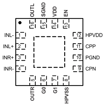
5 Pin Configuration and Functions
RTE (WQFN) Package
(Top View)

Pin Functions
| PIN | I/O/P | DESCRIPTION | |
|---|---|---|---|
| NAME | NO. | ||
| INL- | 1 | I | Inverting left input for differential signals; left input for single-ended signals |
| INL+ | 2 | I | Non-inverting left input for differential signals. Connect to ground for single-ended input applications |
| INR+ | 3 | I | Non-inverting right input for differential signals. Connect to ground for single-ended input applications |
| INR- | 4 | I | Inverting right input for differential signals; right input for single-ended signals |
| OUTR | 5 | O | Right headphone amplifier output. Connect to right terminal of headphone jack |
| G0 | 6 | I | Gain select |
| GAIN0 | I | ||
| G1 | 7 | I | Gain select |
| GAIN1 | I | ||
| HPVSS | 8 | P | Charge pump output and negative power supply for output amplifiers; connect 1μF capacitor to GND |
| CPN | 9 | P | Charge pump negative flying cap. Connect to negative side of 1μF capacitor between CPP and CPN |
| PGND | 10 | P | Ground |
| CPP | 11 | P | Charge pump positive flying cap. Connect to positive side of 1μF capacitor between CPP and CPN |
| HPVDD | 12 | P | Positive power supply for headphone amplifiers. Connect to a 2.2μF capacitor. Do not connect to VDD |
| EN | 13 | I | Amplifier enable. Connect to logic low to shutdown; connect to logic high to activate |
| VDD | 14 | P | Positive power supply for TPA6132A2 |
| SGND | 15 | P | Amplifier reference voltage. Connect to ground terminal of headphone jack |
| OUTL | 16 | O | Left headphone amplifier output. Connect to left terminal of headphone jack |
| Thermal Pad | – | Solder the exposed metal pad on the TPA6132A2RTE QFN package to the landing pad on the PCB. Connect the landing pad to ground or leave it electrically unconnected (floating). | |