SLOS597B December 2008 – July 2017 TPA6132A2
PRODUCTION DATA.
- 1 Features
- 2 Applications
- 3 Description
- 4 Revision History
- 5 Pin Configuration and Functions
- 6 Specifications
- 7 Detailed Description
- 8 Application and Implementation
- 9 Power Supply Recommendations
- 10Layout
- 11Device and Documentation Support
- 12Mechanical, Packaging, and Orderable Information
Package Options
Refer to the PDF data sheet for device specific package drawings
Mechanical Data (Package|Pins)
- RTE|16
Thermal pad, mechanical data (Package|Pins)
- RTE|16
Orderable Information
6 Specifications
6.1 Absolute Maximum Ratings
over operating free-air temperature range, TA = 25°C (unless otherwise noted)| MIN | MAX | UNIT | |||
|---|---|---|---|---|---|
| Supply voltage | VDD | –0.3 | 6 | V | |
| Headphone amplifier supply voltage | HPVDD (do not connect to external supply) | –0.3 | 1.9 | V | |
| Input voltage, VI | INR+, INR-, INL+, INL- | HPVSS –0.3 | HPVDD + 0.3 | V | |
| EN, G0, G1 | –0.3 | VDD + 0.3 | V | ||
| Output continuous total power dissipation | See Thermal Information | ||||
| Operating free-air temperature range, TA | –40 | 85 | °C | ||
| Operating junction temperature range, TJ | –40 | 150 | °C | ||
| Storage temperature range, Tstg | –65 | 85 | °C | ||
6.2 ESD Ratings
| VALUE | UNIT | ||||
|---|---|---|---|---|---|
| V(ESD) | Electrostatic discharge | Human body model (HBM), per ANSI/ESDA/JEDEC JS-001, all pins(1) | OUTL, OUTR | ±8000 | V |
| All Other Pins | ±2000 | ||||
| Charged device model (CDM), per JEDEC specification JESD22-C101, all pins(2) | ±1500 | V | |||
(1) JEDEC document JEP155 states that 500-V HBM allows safe manufacturing with a standard ESD control process.
(2) JEDEC document JEP157 states that 250-V CDM allows safe manufacturing with a standard ESD control process.
6.3 Recommended Operating Condtions
6.4 Thermal Information
| THERMAL METRIC(1) | RTE | UNIT | |
|---|---|---|---|
| 16 PINS | |||
| RθJA | Junction-to-ambient thermal resistance | 51.1 | °C/W |
| RθJC(top) | Junction-to-case (top) thermal resistance | 53.9 | |
| RθJB | Junction-to-board thermal resistance | 24.3 | |
| ψJT | Junction-to-top characterization parameter | 0.9 | |
| ψJB | Junction-to-board characterization parameter | 24.3 | |
| RθJC(bot) | Junction-to-case (bottom) thermal resistance | 9.0 | |
(1) For more information about traditional and new thermal metrics, see the Semiconductor and IC Package Thermal Metrics application report.
6.5 Electrical Characteristics
TA = 25°C (unless otherwise noted)| PARAMETER | TEST CONDITIONS | MIN | TYP | MAX | UNIT |
|---|---|---|---|---|---|
| Output offset voltage | –0.5 | 0.5 | mV | ||
| Power supply rejection ratio | VDD = 2.3 V to 5.5 V | 100 | dB | ||
| High-level output current (EN, G0, G1) | 1 | µA | |||
| Low-level output current (EN, G0, G1) | 1 | µA | |||
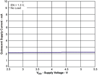
| Supply Current | VDD = 2.3 V, No load, EN = VDD | 2.1 | 3.1 | mA | |
| VDD = 3.6 V, No load, EN = VDD | 2.1 | 3.1 | |||
| VDD = 5.5 V, No load, EN = VDD | 2.2 | 3.2 | |||
| EN = 0 V, VDD = 2.3 V to 5.5 V | 0.7 | 1.2 | µA |
6.6 Operating Characteristics
VDD = 3.6 V , TA = 25°C, RL = 16 Ω (unless otherwise noted)| PARAMETER | TEST CONDITIONS | MIN | TYP | MAX | UNIT | |
|---|---|---|---|---|---|---|
| PO | Output power(1) (Outputs in phase) | THD = 1%, f = 1 kHz | 25 | mW | ||
| THD = 1%, f = 1 kHz, RL = 32 Ω | 22 | |||||
| VO | Output voltage (1) (Outputs in phase) | THD = 1%, VDD = 3.6 V, f = 1 kHz, RL = 100 Ω | 1.1 | VRMS | ||
| AV | Closed-loop voltage gain (OUT / IN–) | G0 = 0 V, G1 = 0 V, (–6 dB) | –0.45 | –0.5 | –0.55 | V/V |
| G0 ≥ 1.3 V, G1 = 0 V, (0 dB) | –0.95 | –1.0 | –1.05 | |||
| G0 = 0 V, G1 ≥ 1.3 V, (3 dB) | –1.36 | –1.41 | –1.46 | |||
| G0 ≥ 1.3 V, G1 ≥ 1.3 V, (6 dB) | –1.95 | –2.0 | –2.05 | |||
| ΔAv | Gain matching | Between Left and Right channels | 1% | |||
| RIN | Input impedance (per input pin) | G0 = 0 V, G1 = 0 V, (–6 dB) | 26.4 | kΩ | ||
| G0 ≥ 1.3 V, G1 = 0 V, (0 dB) | 19.8 | |||||
| G0 = 0 V, G1 ≥ 1.3 V, (3 dB) | 16.5 | |||||
| G0 ≥ 1.3 V, G1 ≥ 1.3 V, (6 dB) | 13.2 | |||||
| Input impedance in shutdown (per input pin) |
EN = 0 V | 10 | ||||
| VCM | Input common-mode voltage range | –0.5 | 1.5 | V | ||
| Output impedance in shutdown | 20 | Ω | ||||
| Input-to-output attenuation in shutdown | EN = 0 V | 80 | dB | |||
| kSVR | AC-power supply rejection ratio | 200 mVpp ripple, f = 217 Hz | -100 | dB | ||
| 200 mVpp ripple, f = 10 kHz | -90 | |||||
| THD+N | Total harmonic distortion plus noise(2) | PO = 20 mW, f = 1 kHz | 0.02% | |||
| PO = 25 mW into 32 Ω, VDD = 5.5 V, f = 1 kHz | 0.01% | |||||
| SNR | Signal-to-noise ratio | PO = 20 mW; G0 ≥ 1.3 V, G1 = 0 V, (AV = 0 dB) | 100 | dB | ||
| En | Noise output voltage | A-weighted | 5.5 | μVRMS | ||
| fosc | Charge pump switching frequency | 1200 | 1275 | 1350 | kHz | |
| tON | Start-up time from shutdown | 5 | ms | |||
| Crosstallk | PO = 20 mW, f = 1 kHz | –80 | dB | |||
| Thermal shutdown | Threshold | 150 | °C | |||
| Hysteresis | 20 | °C | ||||
(1) Per output channel
(2) A-weighted
6.7 Typical Characteristics
TA = 25°C, VDD = 3.6 V, Gain = 0 dB, EN = 3.6 V, CHPVDD = CHPVSS = 2.2 μF, CINPUT = CFLYING = 1 μF, Outputs in Phase
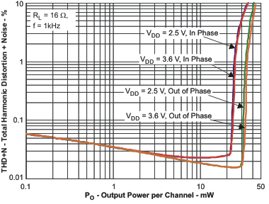 Figure 1. Total Harmonic Distortion + Noise vs
 Output Power
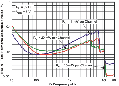
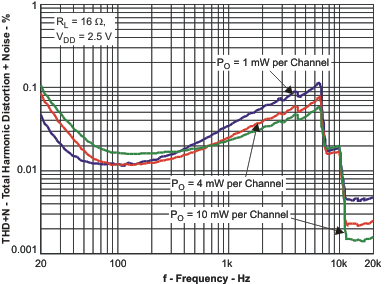 Figure 3. Total Harmonic Distortion + Noise vs Frequency
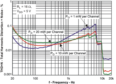 Figure 5. Total Harmonic Distortion + Noise vs Frequency
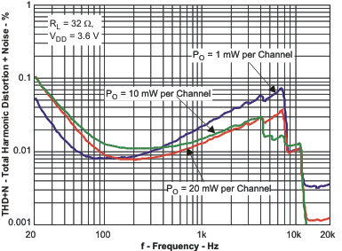
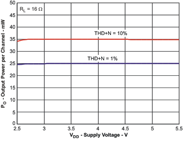
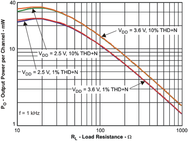
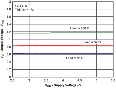
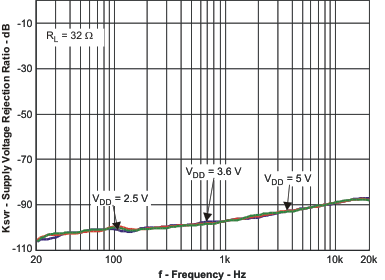
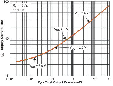
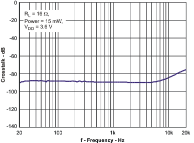
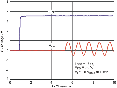
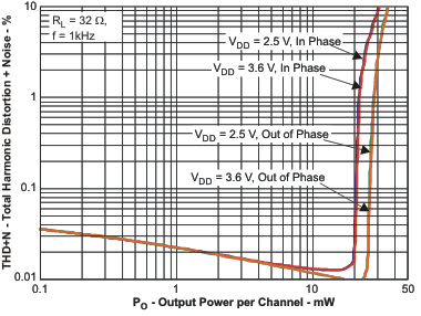 Figure 2. Total Harmonic Distortion + Noise vs
 Output Power
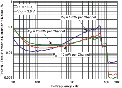 Figure 4. Total Harmonic Distortion + Noise vs Frequency
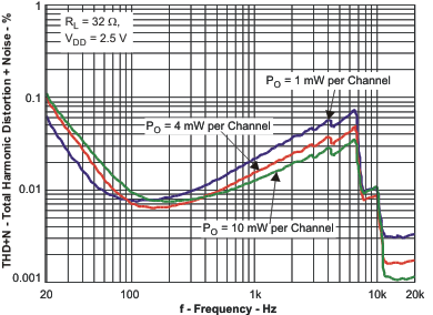 Figure 6. Total Harmonic Distortion + Noise vs Frequency
