SLOS821B June 2013 – September 2014 TPA6133A2
PRODUCTION DATA.
- 1 Features
- 2 Applications
- 3 Description
- 4 Simplified Application Diagram
- 5 Revision History
- 6 Pin Configuration and Functions
- 7 Specification
- 8 Detailed Description
- 9 Application and Implementation
- 10Power Supply Recommendations
- 11Layout
- 12Device and Documentation Support
- 13Mechanical, Packaging, and Orderable Information
Package Options
Mechanical Data (Package|Pins)
- RTJ|20
Thermal pad, mechanical data (Package|Pins)
- RTJ|20
Orderable Information
7 Specification
7.1 Absolute Maximum Ratings(1)
over operating free-air temperature range, TA = 25°C (unless otherwise noted)| MIN | MAX | UNIT | |||
|---|---|---|---|---|---|
| Supply voltage, VDD | –0.3 | 6 | V | ||
| Input voltage | RIGHTINx, LEFTINx | CPVSS-0.2 V to minimum of (3.6 V, VDD+0.2 V) |
|||
| SD, TEST1, TEST2 | –0.3 | 7 | V | ||
| Output continuous total power dissipation | See the Thermal Information Table | ||||
| Operating free-air temperature range, TA | –40 | 85 | °C | ||
| Operating junction temperature range, TJ | –40 | 150 | °C | ||
(1) Stresses beyond those listed under absolute maximum ratings may cause permanent damage to the device. These are stress ratings only, and functional operation of the device at these or any other conditions beyond those indicated under recommended operating conditions is not implied. Exposure to absolute-maximum-rated conditions for extended periods may affect device reliability.
7.2 Handling Ratings
| MIN | MAX | UNIT | |||
|---|---|---|---|---|---|
| Tstg | Storage temperature range | –65 | 150 | °C | |
| V(ESD) | Electrostatic discharge | Human body model (HBM), per ANSI/ESDA/JEDEC JS-001, all pins(1) | –3 | 3 | kV |
| Charged device model (CDM), per JEDEC specification JESD22-C101, all pins(2) | –750 | 750 | V | ||
(1) JEDEC document JEP155 states that 500-V HBM allows safe manufacturing with a standard ESD control process.
(2) JEDEC document JEP157 states that 250-V CDM allows safe manufacturing with a standard ESD control process.
7.3 Recommended Operating Conditions
7.4 Thermal Information
| THERMAL METRIC(1) | RTJ | UNIT | |
|---|---|---|---|
| 20 PINS | |||
| RθJA | Junction-to-ambient thermal resistance | 34.8 | °C/W |
| RθJC(top) | Junction-to-case (top) thermal resistance | 32.5 | |
| RθJB | Junction-to-board thermal resistance | 11.6 | |
| ψJT | Junction-to-top characterization parameter | 0.4 | |
| ψJB | Junction-to-board characterization parameter | 11.6 | |
| RθJC(bot) | Junction-to-case (bottom) thermal resistance | 3.1 | |
(1) For more information about traditional and new thermal metrics, see the IC Package Thermal Metrics application report, SPRA953.
7.5 Electrical Characteristics
TA = 25°C (unless otherwise noted)| PARAMETER | TEST CONDITIONS | MIN | TYP | MAX | UNIT | ||
|---|---|---|---|---|---|---|---|
| |VOS| | Output offset voltage | VDD = 2.5 V to 5.5 V, inputs grounded | 135 | 400 | μV | ||
| PSRR | DC Power supply rejection ratio | VDD = 2.5 V to 5.5 V, inputs grounded | –101 | -85 | dB | ||
| CMRR | Common mode rejection ratio | VDD = 2.5 V to 5.5 V | –69 | dB | |||
| |IIH| | High-level input current | VDD = 5.5 V, VI = VDD | TEST1, TEST2 | 1 | µA | ||
| SD | 10 | ||||||
| |IIL| | Low-level input current | VDD = 5.5 V, VI = 0 V | SD | 1 | µA | ||
| IDD | Supply current | VDD = 2.5 V to 5.5 V, SD = VDD | 4.2 | 6 | mA | ||
| Shutdown mode, VDD = 2.5V to 5.5 V, SD = 0 V | 0.08 | 1 | µA | ||||
7.6 Operating Characteristics
VDD = 3.6 V , TA = 25°C, RL = 16 Ω (unless otherwise noted)| PARAMETER | TEST CONDITIONS | MIN | TYP | MAX | UNIT | ||
|---|---|---|---|---|---|---|---|
| PO | Output power | Stereo, Outputs out of phase, THD = 1%, f = 1 kHz, Gain = +4 dB |
VDD = 2.5V | 63 | mW | ||
| VDD = 3.6V | 133 | ||||||
| VDD = 5V | 142 | ||||||
| THD+N | Total harmonic distortion plus noise | PO = 35 mW | f = 100 Hz | 0.0096% | |||
| f = 1 kHz | 0.007% | ||||||
| f = 20 kHz | 0.0021% | ||||||
| kSVR | Supply ripple rejection ratio | 200 mVpp ripple, f = 217 Hz | -94.3 | -85 | dB | ||
| 200 mVpp ripple, f = 1 kHz | -92 | ||||||
| 200 mVpp ripple, f = 20 kHz | -77.1 | ||||||
| Av | Channel DC Gain | SD = VDD | 1.597 | V/V | |||
| ΔAv | Gain matching | 0.1% | |||||
| Slew rate | 0.4 | V/µs | |||||
| Vn | Noise output voltage | VDD = 3.6V, A-weighted, Gain = +4 dB | 12 | µVRMS | |||
| fosc | Charge pump switching frequency | 300 | 381 | 500 | kHz | ||
| Start-up time from shutdown | 4.8 | ms | |||||
| Differential input impedance | 36.6 | kΩ | |||||
| SNR | Signal-to-noise ratio | Po = 35 mW | 93 | dB | |||
| Thermal shutdown | Threshold | 180 | °C | ||||
| Hysteresis | 35 | °C | |||||
| ZO | HW Shutdown HP output impedance | SD = 0 V, measured output to ground. | 112 | Ω | |||
| CO | Output capacitance | 80 | pF | ||||
7.7 Typical Characteristics
Table 1. Table of Graphs
| Figure | ||
|---|---|---|
| Total harmonic distortion + noise | versus Output power | Figure 1–Figure 4 |
| Total harmonic distortion + noise | versus Frequency | Figure 5–Figure 12 |
| Supply voltage rejection ratio | versus Frequency | Figure 13-Figure 14 |
| Common mode rejection ratio | versus Frequency | Figure 15-Figure 16 |
| Crosstalk | versus Frequency | Figure 17-Figure 18 |
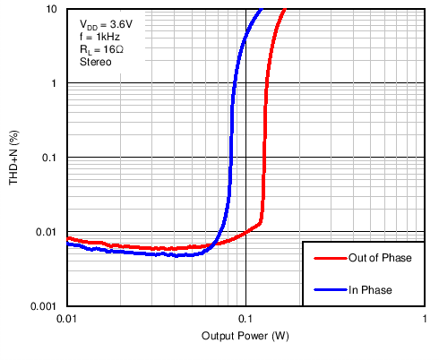 Figure 1. Total Harmonic Distortion + Noise vs Output Power
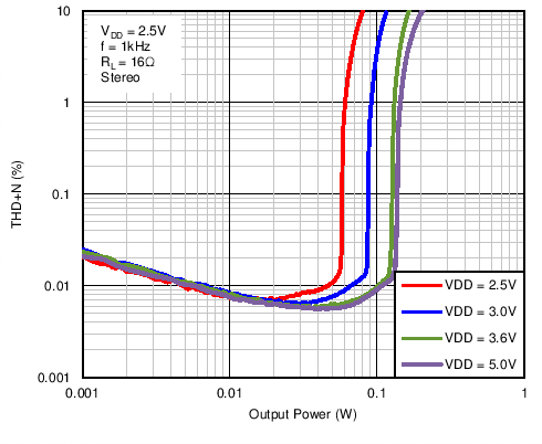 Figure 3. Total Harmonic Distortion + Noise vs Output Power
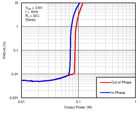 Figure 2. Total Harmonic Distortion + Noise vs Output Power
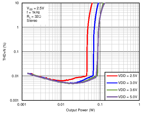 Figure 4. Total Harmonic Distortion + Noise vs Output Power
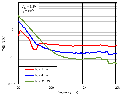 Figure 5. Total Harmonic Distortion + Noise vs Frequency
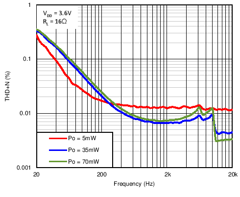 Figure 7. Total Harmonic Distortion + Noise vs Frequency
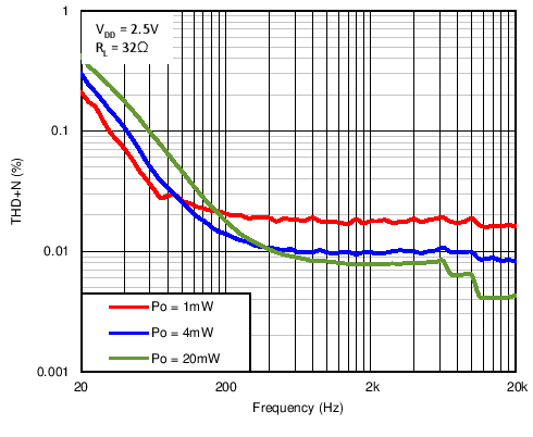 Figure 9. Total Harmonic Distortion + Noise vs Frequency
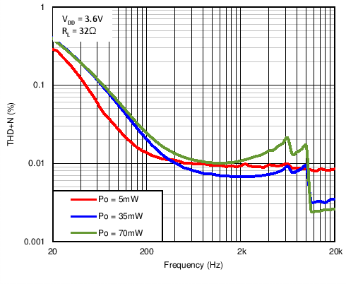 Figure 11. Total Harmonic Distortion + Noise vs Frequency
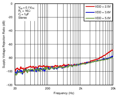 Figure 13. Supply Voltage Rejection Ratio vs Frequency
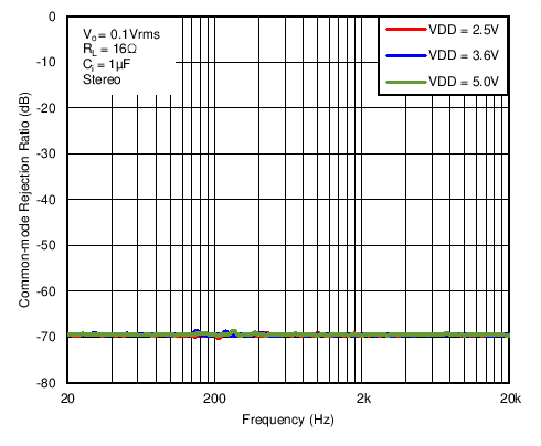 Figure 15. Common Mode Rejection Ratio vs Frequency
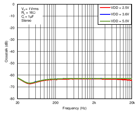 Figure 17. Crosstalk vs Frequency
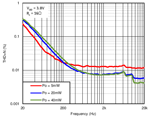 Figure 6. Total Harmonic Distortion + Noise vs Frequency
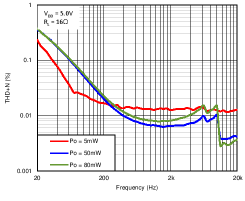 Figure 8. Total Harmonic Distortion + Noise vs Frequency
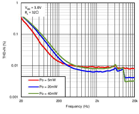 Figure 10. Total Harmonic Distortion + Noise vs Frequency
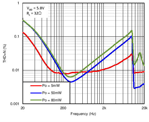 Figure 12. Total Harmonic Distortion + Noise vs Frequency
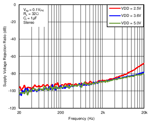 Figure 14. Supply Voltage Rejection Ratio vs Frequency
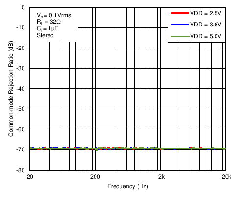 Figure 16. Common Mode Rejection Ratio vs Frequency
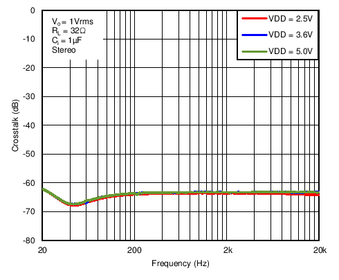 Figure 18. Crosstalk vs Frequency