SLOS704B January 2011 – August 2015 TPA6138A2
PRODUCTION DATA.
- 1 Features
- 2 Applications
- 3 Description
- 4 Revision History
- 5 Device Comparison Table
- 6 Pin Configuration and Functions
- 7 Specifications
- 8 Parameter Measurement Information
- 9 Detailed Description
- 10Application and Implementation
- 11Power Supply Recommendations
- 12Layout
- 13Device and Documentation Support
- 14Mechanical, Packaging, and Orderable Information
Package Options
Mechanical Data (Package|Pins)
- PW|14
Thermal pad, mechanical data (Package|Pins)
Orderable Information
10 Application and Implementation
NOTE
Information in the following applications sections is not part of the TI component specification, and TI does not warrant its accuracy or completeness. TI’s customers are responsible for determining suitability of components for their purposes. Customers should validate and test their design implementation to confirm system functionality.
10.1 Application Information
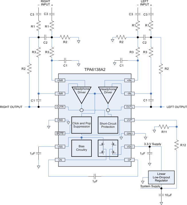
The TPA6138A2 starts its operation by asserting the MUTE pin to logic 1. The device enters in mute mode when pulling low MUTE pin. The charge pump generates a negative supply voltage. The charge pump flying capacitor connected between CP and CN transfers charge to generate the negative supply voltage. The output voltages are capable of positive and negative voltage swings and are centered close to 0 V, eliminating the need for output capacitors. Input coupling capacitors block any dc bias from the audio source and ensure maximum dynamic range. The device has built-in pop suppression circuitry to completely eliminate pop noise during turn- on, turn-off and enter or exit shutdown mode.
10.1.1 Gain-Setting Resistor Ranges
The gain-setting resistors, RIN and Rfb, must be chosen so that noise, stability, and input capacitor size of the TPA6138A2 are kept within acceptable limits. Voltage gain is defined as Rfb divided by RIN.
Selecting values that are too low demands a large input ac-coupling capacitor, CIN. Selecting values that are too high increases the noise of the amplifier. Table 1 lists the recommended resistor values for different inverting-input gain settings.
Table 1. Recommended Resistor Values
| GAIN | INPUT RESISTOR VALUE, RIN | FEEDBACK RESISTOR VALUE, Rfb |
|---|---|---|
| –1 V/V | 10 kΩ | 10 kΩ |
| –1.5 V/V | 8.2 kΩ | 12 kΩ |
| –2 V/V | 15 kΩ | 30 kΩ |
| –10 V/V | 4.7 kΩ | 47 kΩ |
10.1.2 Input-Blocking Capacitors
DC input-blocking capacitors are required to be added in series with the audio signal into the input pins of the TPA6138A2. These capacitors block the dc portion of the audio source and allow the TPA6138A2 inputs to be properly biased to provide maximum performance.
These capacitors form a high-pass filter with the input resistor, RIN. The cutoff frequency is calculated using Equation 5. For this calculation, the capacitance used is the input-blocking capacitor and the resistance is the input resistor chosen from Table 1; then the frequency and/or capacitance can be determined when one of the two values is given.
It is recommended to use electrolytic capacitors or high-voltage-rated capacitors as input blocking capacitors to ensure minimal variation in capacitance with input voltages. Such variation in capacitance with input voltages is commonly seen in ceramic capacitors and can increase low-frequency audio distortion.

10.2 Typical Application

10.2.1 Design Requirements
This typical application requires the parameters listed in Table 2.
Table 2. Design Parameters
| PARAMETER | VALUES |
|---|---|
| Input voltage range | 3 V to 3.6 V |
| Current | 14 mA to 25 mA |
10.2.2 Detailed Design Procedure
10.2.2.1 Charge-Pump Flying Capacitor and VSS Capacitor
The charge-pump flying capacitor serves to transfer charge during the generation of the negative supply voltage. The VSS capacitor must be at least equal to the charge-pump capacitor in order to allow maximum charge transfer. Low-ESR capacitors are an ideal selection, and a value of 1 μF is typical. Capacitor values that are smaller than 1 μF can be used, but the maximum output voltage may be reduced, and the device may not operate to specifications. If the TPA6138A2 is used in highly noise-sensitive circuits, it is recommended to add a small LC filter on the VDD connection.
10.2.2.2 Decoupling Capacitors
The TPA6138A2 is a DirectPath headphone amplifier that requires adequate power-supply decoupling to ensure that the noise and total harmonic distortion (THD) are low. A good low equivalent-series-resistance (ESR) ceramic capacitor, typically 1 μF, placed as close as possible to the device VDD lead works best. Placing this decoupling capacitor close to the TPA6138A2 is important for the performance of the amplifier. For filtering lower-frequency noise signals, a 10-μF or greater capacitor placed near the audio power amplifier would also help, but it is not required in most applications because of the high PSRR of this device.
10.2.3 Application Curves
See the curves listed in Table 3 for the application curves.
Table 3. Table of Graphs
| FIGURE | ||
|---|---|---|
| Total Harmonic Distortion and Noise vs Output Power | Figure 1 | |
| Total Harmonic Distortion and Noise vs Output Voltage | Figure 2 | |
| Total Harmonic Distortion and Noise vs Frequency | Figure 3 | |
| Total Harmonic Distortion and Noise vs Frequency | Figure 4 | |
| Crosstalk vs Frequency | Figure 5 | |
| Supply Rejection Ratio vs Frequency | Figure 6 | |