SBOS555G June 2011 – May 2024 TPA6211A1-Q1
PRODUCTION DATA
- 1
- 1 Features
- 2 Applications
- 3 Description
- 4 Pin Configuration and Functions
- 5 Specifications
- 6 Detailed Description
-
7 Application and Implementation
- 7.1 Application Information
- 7.2
Typical Applications
- 7.2.1
Typical Differential Input Application
- 7.2.1.1 Design Requirements
- 7.2.1.2 Detailed Design Procedure
- 7.2.1.3 Application Curves
- 7.2.2 Other Application Circuits
- 7.2.1
Typical Differential Input Application
- 7.3 Power Supply Recommendations
- 7.4 Layout
- 8 Device and Documentation Support
- 9 Revision History
- 10Mechanical, Packaging, and Orderable Information
Package Options
Mechanical Data (Package|Pins)
- DGN|8
Thermal pad, mechanical data (Package|Pins)
- DGN|8
Orderable Information
7.2.1.2.4.2 Step 2: High-Pass Filter
Equation 26. 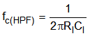
Because the application in this case requires a gain of 4 V/V, RI must be set to 10 kΩ.
Substituting RI into Equation 26.
Equation 27. 
Therefore,
Equation 28. 
Substituting 100 Hz for fc(HPF) and solving for CI:
Equation 29. CI = 0.16 µF
At this point, a first-order band-pass filter has been created with the low-frequency cutoff set to 100 Hz and the high-frequency cutoff set to 10 kHz.
The process can be taken a step further by creating a second-order high-pass filter. This is accomplished by placing a resistor (Ra) and capacitor (Ca) in the input path. Ra must be at least 10 times smaller than RI; otherwise its value has a noticeable effect on the gain, as Ra and RI are in series.