SLVS640F October 2007 – February 2015 TPD12S520
PRODUCTION DATA.
- 1 Features
- 2 Applications
- 3 Description
- 4 Revision History
- 5 Pin Configuration and Functions
- 6 Specifications
-
7 Detailed Description
- 7.1 Overview
- 7.2 Functional Block Diagram
- 7.3
Feature Description
- 7.3.1 ±8-kV Contact ESD Protection on External Lines
- 7.3.2 Single-Chip ESD Solution for HDMI Driver
- 7.3.3 Supports All HDMI 1.3 and HDMI 1.4b Data Rates
- 7.3.4 38-Pin TSSOP Provides Seamless Layout Option With HDMI Connector
- 7.3.5 24-Pin WQFNPackage for Space Constrained Applications
- 7.3.6 Integrated Level Shifting for the Control Lines
- 7.3.7 Backdrive Protection
- 7.3.8 Lead-Free Package
- 7.4 Device Functional Modes
- 8 Application and Implementation
- 9 Power Supply Recommendations
- 10Layout
- 11Device and Documentation Support
- 12Mechanical, Packaging, and Orderable Information
Package Options
Mechanical Data (Package|Pins)
Thermal pad, mechanical data (Package|Pins)
Orderable Information
5 Pin Configuration and Functions
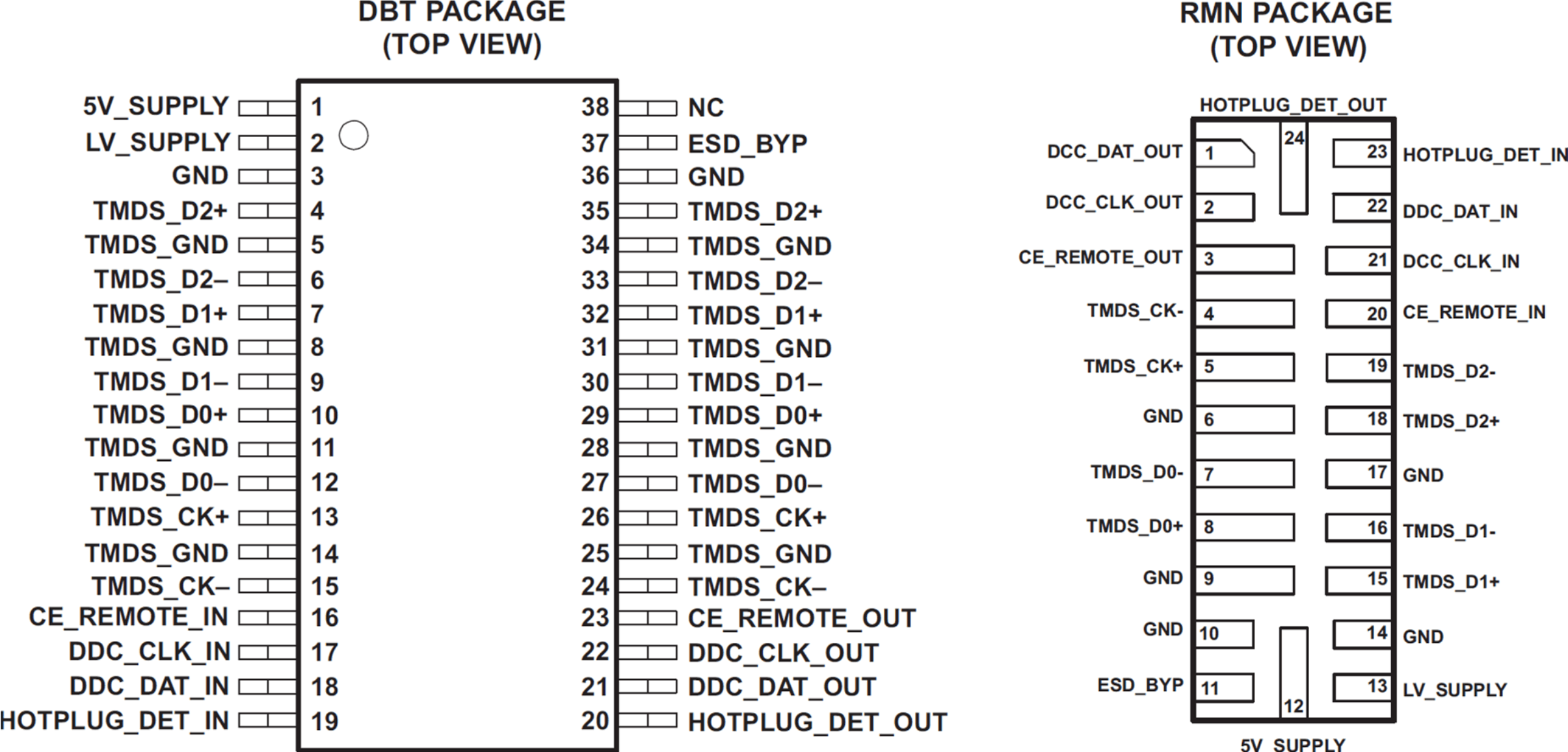
Pin Functions
| NAME | PIN NO. | TYPE | ESD LEVEL | DESCRIPTION | |
|---|---|---|---|---|---|
| DBT | RMN | ||||
| 5V_SUPPLY | 1 | 12 | PWR | 2 kV(4) | Bias for TMDS protection |
| LV_SUPPLY | 2 | 13 | PWR | 2 kV(4) | Bias for CE/DDC/HOTPLUG level shifters |
| GND, TMDS_GND | 3, 5, 8, 11,14, 25, 28, 31, 34, 36 |
6, 9, 10, 14, 17 | GND | NA | TMDS ESD and parasitic GND return(5) |
| TMDS_D2+ | 4, 35 | 18 | IO | 8 kV(3) | TMDS 0.8-pF ESD protection(1) |
| TMDS_D2– | 6, 33 | 19 | IO | 8 kV(3) | TMDS 0.8-pF ESD protection(1) |
| TMDS_D1+ | 7, 32 | 15 | IO | 8 kV(3) | TMDS 0.8-pF ESD protection(1) |
| TMDS_D1– | 9, 30 | 16 | IO | 8 kV(3) | TMDS 0.8-pF ESD protection(1) |
| TMDS_D0+ | 10, 29 | 8 | IO | 8 kV(3) | TMDS 0.8-pF ESD protection(1) |
| TMDS_D0– | 12, 27 | 7 | IO | 8 kV(3) | TMDS 0.8-pF ESD protection(1) |
| TMDS_CK+ | 13, 26 | 5 | IO | 8 kV(3) | TMDS 0.8-pF ESD protection(1) |
| TMDS_CK– | 15, 24 | 4 | IO | 8 kV(3) | TMDS 0.8-pF ESD protection(1) |
| CE_REMOTE_IN | 16 | 20 | IO | 2 kV(4) | LV_SUPPLY referenced logic level into ASIC |
| DDC_CLK_IN | 17 | 21 | IO | 2 kV(4) | LV_SUPPLY referenced logic level into ASIC |
| DDC_DAT_IN | 18 | 22 | IO | 2 kV(4) | LV_SUPPLY referenced logic level into ASIC |
| HOTPLUG_DET_IN | 19 | 23 | IO | 2 kV(4) | LV_SUPPLY referenced logic level into ASIC |
| HOTPLUG_DET_OUT | 20 | 24 | IO | 8 kV(3) | 5 V_SUPPLY referenced logic level out, plus 3.5-pF ESD(2) to connector |
| DDC_DAT_OUT | 21 | 1 | IO | 8 kV(3) | 5 V_SUPPLY referenced logic level out, plus 3.5-pF ESD to connector |
| DDC_CLK_OUT | 22 | 2 | IO | 8 kV(3) | 5 V_SUPPLY referenced logic level out, plus 3.5-pF ESD to connector |
| CE_REMOTE_OUT | 23 | 3 | IO | 8 kV(3) | 5 V_SUPPLY referenced logic level out, plus 3.5-pF ESD to connector |
| ESD_BYP | 37 | 11 | IO | 2 kV(4) | ESD bypass. This pin must be connected to a 0.1-μF ceramic capacitor. |
| NC | 38 | NA | No connection | ||
(1) These two pins must be connected together inline on the PCB.
(2) This output can be connected to an external 0.1-μF ceramic capacitor, resulting in an increased ESD withstand voltage rating.
(3) Standard IEC 61000-4-2, CDISCHARGE = 150 pF, RDISCHARGE = 330 Ω, 5V_SUPPLY and LV_SUPPLY within recommended operating conditions, GND = 0 V, and ESD_BYP (pin 37) and HOTPLUG_DET_OUT (pin 20) each bypassed with a 0.1-μF ceramic capacitor connected to GND.
(4) Human body model (HBM) per MIL-STD-883, Method 3015, CDISCHARGE = 100 pF, RDISCHARGE = 1.5 kΩ, 5V_SUPPLY and LV_SUPPLY within recommended operating conditions, GND = 0 V, and ESD_BYP (pin 37) and HOTPLUG_DET_OUT (pin 20) each bypassed with a 0.1-μF ceramic capacitor connected to GND.
(5) These pins should be routed directly to the associated GND pins on the HDMI connector, with single-point ground vias at the connector.