SLVS640F October 2007 – February 2015 TPD12S520
PRODUCTION DATA.
- 1 Features
- 2 Applications
- 3 Description
- 4 Revision History
- 5 Pin Configuration and Functions
- 6 Specifications
-
7 Detailed Description
- 7.1 Overview
- 7.2 Functional Block Diagram
- 7.3
Feature Description
- 7.3.1 ±8-kV Contact ESD Protection on External Lines
- 7.3.2 Single-Chip ESD Solution for HDMI Driver
- 7.3.3 Supports All HDMI 1.3 and HDMI 1.4b Data Rates
- 7.3.4 38-Pin TSSOP Provides Seamless Layout Option With HDMI Connector
- 7.3.5 24-Pin WQFNPackage for Space Constrained Applications
- 7.3.6 Integrated Level Shifting for the Control Lines
- 7.3.7 Backdrive Protection
- 7.3.8 Lead-Free Package
- 7.4 Device Functional Modes
- 8 Application and Implementation
- 9 Power Supply Recommendations
- 10Layout
- 11Device and Documentation Support
- 12Mechanical, Packaging, and Orderable Information
Package Options
Mechanical Data (Package|Pins)
Thermal pad, mechanical data (Package|Pins)
Orderable Information
6 Specifications
6.1 Absolute Maximum Ratings(1)
over operating free-air temperature range (unless otherwise noted)| MIN | MAX | UNIT | |||
|---|---|---|---|---|---|
| V5V_SUPPLY | Supply voltage | –0.3 | 6 | V | |
| VLV_SUPPLY | |||||
| VI/O | DC voltage at any channel input | –0.5 | 6 | V | |
| TA | Operating Free Air Temperature | –40 | 85 | °C | |
| Tstg | Storage temperature range | –65 | 150 | °C | |
(1) Stresses beyond those listed under Absolute Maximum Ratings may cause permanent damage to the device. These are stress ratings only, and functional operation of the device at these or any other conditions beyond those indicated under Recommended Operating Conditions is not implied. Exposure to absolute-maximum-rated conditions for extended periods may affect device reliability.
6.2 ESD Ratings
| VALUE | UNIT | ||||
|---|---|---|---|---|---|
| V(ESD) | Electrostatic discharge | Human body model (HBM), per MIL-STD-883, Method 3015, CDISCHARGE = 100 pF, RDISCHARGE = 1.5 kΩ(1) | See Pin Configuration and Functions | ±2000 | V |
| IEC 61000-4-2 Contact Discharge(2) | See Pin Configuration and Functions | ±8000 | |||
(1) JEDEC document JEP155 states that 500-V HBM allows safe manufacturing with a standard ESD control process. Manufacturing with less than 500-V HBM is possible with the necessary precautions.
(2) JEDEC document JEP157 states that 250-V CDM allows safe manufacturing with a standard ESD control process. Manufacturing with less than 250-V CDM is possible with the necessary precautions.
6.3 Recommended Operating Conditions
over operating free-air temperature range (unless otherwise noted)| MIN | TYP | MAX | UNIT | |||
|---|---|---|---|---|---|---|
| TA | Operating free-air temperature | –40 | 85 | °C | ||
| 5V_SUPPLY | Operating supply voltage | GND | 5 | 5.5 | V | |
| LV_SUPPLY | Bias supply voltage | 1 | 3.3 | 5.5 | V | |
6.4 Thermal Information
| THERMAL METRIC(1) | TPD12S520 | UNIT | ||
|---|---|---|---|---|
| DBT | RMN | |||
| 38 PINS | 24 PINS | |||
| RθJA | Junction-to-ambient thermal resistance | 83.6 | 80.8 | °C/W |
| RθJC(top) | Junction-to-case (top) thermal resistance | 29.8 | 36.4 | |
| RθJB | Junction-to-board thermal resistance | 44.7 | 27.1 | |
| ψJT | Junction-to-top characterization parameter | 2.9 | 1.4 | |
| ψJB | Junction-to-board characterization parameter | 44.1 | 27.0 | |
(1) For more information about traditional and new thermal metrics, see the IC Package Thermal Metrics application report, SPRA953.
6.5 Electrical Characteristics
over operating free-air temperature range (unless otherwise noted)| PARAMETER | TEST CONDITIONS | MIN | TYP | MAX | UNIT | ||||
|---|---|---|---|---|---|---|---|---|---|
| I5V | Operating supply current | 5V_SUPPLY = 5 V | 1 | 5 | µA | ||||
| ILV | Bias supply current | LV_SUPPLY = 3.3 V | 1 | 2 | mA | ||||
| IOFF | OFF-state leakage current, level-shifting NFET | LV_SUPPLY = 0 V | 0.1 | 1 | µA | ||||
| IBACK DRIVE | Current conducted from output pins to V_SUPPLY rails when powered down | 5V_SUPPLY < VCH_OUT | TMDS_D[2:0]+/–, TMDS_CK+/–, CE_REMOTE_OUT, DDC_DAT_OUT, DDC_CLK_OUT, HOTPLUG_DET_OUT |
0.1 | 5 | µA | |||
| VON | Voltage drop across level-shifting NFET when ON | LV_SUPPLY = 2.5 V, VS = GND, IDS = 3 mA | 75 | 95 | 140 | mV | |||
| VF | Diode forward voltage | IF = 8 mA, | Top diode | 1 | V | ||||
| TA = 25°C(1) | Bottom diode | 1 | |||||||
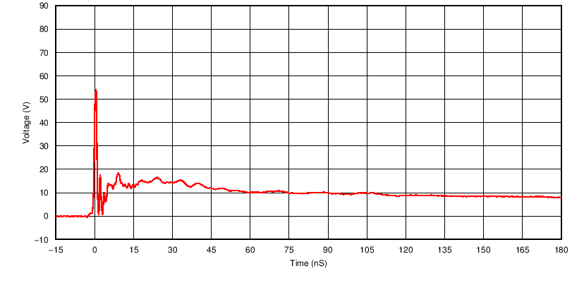
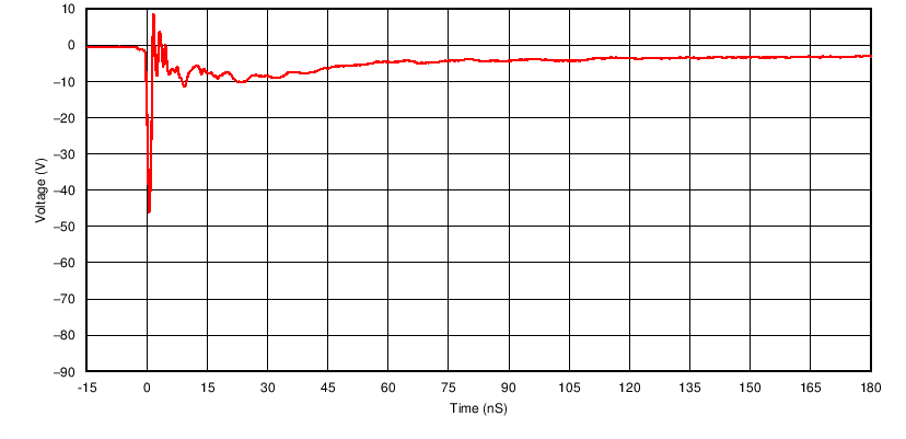
| VCL | Channel clamp voltage at ±8 kV HBM ESD | TA = 25°C(1)(2) | Positive transients | 9 | V | ||||
| Negative transients | -9 | ||||||||
| RDYN | Dynamic resistance | I = 1 A, TA = 25°C(3) | Positive transients | 0.6 | Ω | ||||
| Negative transients | 0.5 | ||||||||
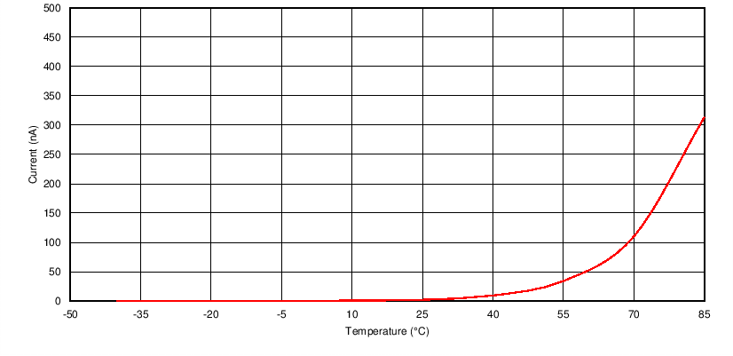
| ILEAK | TMDS channel leakage current | TA = 25°C(1) | 0.01 | 1 | µA | ||||
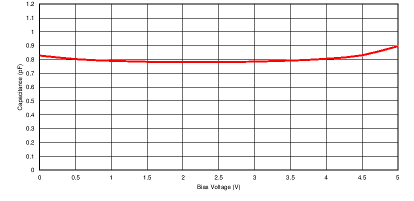
| CIN, TMDS |
TMDS channel input capacitance | 5V_SUPPLY= 5 V, Measured at 1 MHz, VBIAS = 2.5 V(1) |
0.8 | 1.0 | pF | ||||
| ΔCIN, TMDS |
TMDS channel input capacitance matching | 5V_SUPPLY= 5 V, Measured at 1 MHz, | 0.05 | pF | |||||
| CMUTUAL | Mutual capacitance between signal pin and adjacent signal pin | 5V_SUPPLY= 0 V, Measured at 1 MHz, VBIAS = 2.5 V(1) |
0.07 | pF | |||||
| CIN | Level-shifting input capacitance, capacitance to GND | 5V_SUPPLY= 0 V, Measured at 100 KHz, VBIAS = 2.5 V(1) |
DDC | 3.5 | 4 | pF | |||
| CEC | 3.5 | 4 | |||||||
| HP | 3.5 | 4 | |||||||
(1) This parameter is specified by design and verified by device characterization
(2) Human-Body Model (HBM) per MIL-STD-883, Method 3015, CDISCHARGE = 100 pF, RDISCHARGE = 1.5 kΩ
(3) These measurements performed with no external capacitor on ESD_BYP.
(4) Intrapair matching, each TMDS pair (i.e., D+, D–)
