SLVSAM5A January 2011 – April 2016 TPD3F303
PRODUCTION DATA.
- 1 Features
- 2 Applications
- 3 Description
- 4 Revision History
- 5 Pin Configuration and Functions
- 6 Specifications
- 7 Detailed Description
- 8 Application and Implementation
- 9 Power Supply Recommendations
- 10Layout
- 11Device and Documentation Support
- 12Mechanical, Packaging, and Orderable Information
Package Options
Mechanical Data (Package|Pins)
Thermal pad, mechanical data (Package|Pins)
Orderable Information
8 Application and Implementation
NOTE
Information in the following applications sections is not part of the TI component specification, and TI does not warrant its accuracy or completeness. TI’s customers are responsible for determining suitability of components for their purposes. Customers should validate and test their design implementation to confirm system functionality.
8.1 Application Information
The TPD3F303 is a diode type TVS + EMI filter which is used to provide a path to ground for dissipating ESD events on signal lines between a SIM card slot and a system. As the current from ESD passes through the TVS, only a small voltage drop is present across the diode. This is the voltage presented to the protected IC across the termination resistors.
8.2 Typical Application
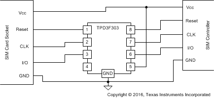 Figure 6. Typical SIM Card Application
8.2.1 Design Requirements
For this design example, one TPD3F303 is used to protect a SIM card interface. Table 1 lists the parameters for Figure 6.
Table 1. Design Parameters
| PARAMETER | VALUE |
|---|---|
| Signal Range on Protected Lines | 0 V to 5 V |
| Required Level of IEC ESD Protection | ±15-kV Contact, ±15-kV Air Gap |
8.2.2 Detailed Design Procedure
To begin the design process, some parameters must be decided upon; the designer must know the following:
- Voltage range of the signal on all protected lines
- Required ESD protection needed
8.2.2.1 Signal Range
The TPD3F303 supports signal ranges from 0 V to 5.5 V, which supports the SIM card application
8.2.2.2 Required ESD Protection
The TPD3F303 is rated to withstand up to ±15-kV contact and ±15-kV air gap IEC ESD. This meets the IEC ESD design target.
8.2.3 Application Curves
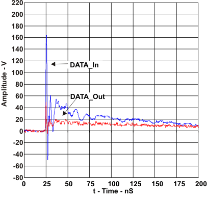 Figure 7. +15-kV IEC Contact, DATA1_In Stressed
 Figure 9. +15-kV IEC Contact, CLK_In Stressed
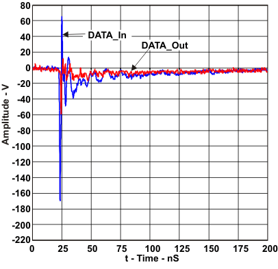 Figure 8. -15-kV IEC Contact, DATA1_In Stressed
 Figure 10. -15-kV IEC Contact, CLK_In Stressed