SLVSCO7C August 2014 – September 2017 TPD1E05U06-Q1 , TPD4E05U06-Q1
PRODUCTION DATA.
- 1 Features
- 2 Applications
- 3 Description
- 4 Revision History
- 5 Pin Configuration and Functions
- 6 Specifications
- 7 Detailed Description
- 8 Application and Implementation
- 9 Layout
- 10Device and Documentation Support
- 11Mechanical, Packaging, and Orderable Information
Package Options
Mechanical Data (Package|Pins)
- DQA|10
Thermal pad, mechanical data (Package|Pins)
- DQA|10
Orderable Information
6 Specifications
6.1 Absolute Maximum Ratings
over operating free-air temperature range (unless otherwise noted) (1)(2)| MIN | MAX | UNIT | ||
|---|---|---|---|---|
| Electrical fast transient | IEC 61000-4-4 (5/50 ns) | 80 | A | |
| Peak pulse | IEC 61000-4-5 Current (tp – 8/20 µs) | 2.5 | A | |
| IEC 61000-4-5 Power (tp – 8/20 µs) - TPD4E05U06-Q1(3) | 40 | W | ||
| IEC 61000-4-5 Power (tp – 8/20 µs) - TPD1E05U06-Q1(3) | 30 | W | ||
| TA | Operating temperature | –40 | 125 | °C |
| Tstg | Storage temperature | –65 | 150 | °C |
(1) Stresses beyond those listed under Absolute Maximum Ratings may cause permanent damage to the device. These are stress ratings only, which do not imply functional operation of the device at these or any other conditions beyond those indicated under Recommended Operating Conditions. Exposure to absolute-maximum-rated conditions for extended periods may affect device reliability.
(2) Voltages are with respect to GND unless otherwise noted.
(3) Measured at 25°C
6.2 ESD Ratings—AEC Specification
| VALUE | UNIT | |||
|---|---|---|---|---|
| V(ESD) | Electrostatic discharge(1) | Human-body model (HBM), per AEC Q100-002(2) | ±8000 | V |
| Charged-device model (CDM), per AEC Q100-011 | ±1000 | |||
(1) Electrostatic discharge (ESD) to measure device sensitivity and immunity to damage caused by assembly line electrostatic discharges into the device.
(2) AEC Q100-002 indicates that HBM stressing shall be in accordance with the ANSI/ESDA/JEDEC JS-001 specification.
6.3 ESD Ratings—IEC Specification
| VALUE | UNIT | |||
|---|---|---|---|---|
| V(ESD) | Electrostatic Discharge | IEC 61000-4-2 contact discharge - TPD4E05U06-Q1 (1) | ±12000 | V |
| IEC 61000-4-2 contact discharge - TPD1E05U06-Q1 | ±12000 | |||
| IEC 61000-4-2 air-gap discharge | ±15000 | |||
(1) Measured at 25°C, per IEC 61000.4.2 Ed. 2.0 Section 7.2.4.
6.4 Recommended Operating Conditions
over operating free-air temperature range (unless otherwise noted)| MIN | MAX | UNIT | ||
|---|---|---|---|---|
| VIO | Input pin voltage | 0 | 5.5 | V |
| TA | Operating free-air temperature | –40 | 125 | °C |
6.5 Thermal Information
| THERMAL METRIC(1) | TPD1E05U06-Q1 | TPD4E05U06-Q1 | UNIT | |
|---|---|---|---|---|
| DPY (X1SON) | DQA (USON) | |||
| 2 PINS | 10 PINS | |||
| RθJA | Junction-to-ambient thermal resistance | 697.3 | 327 | °C/W |
| RθJC(top) | Junction-to-case (top) thermal resistance | 471 | 189.5 | °C/W |
| RθJB | Junction-to-board thermal resistance | 575.9 | 257.7 | °C/W |
| ψJT | Junction-to-top characterization parameter | 175.7 | 60.9 | °C/W |
| ψJB | Junction-to-board characterization parameter | 575.1 | 257 | °C/W |
(1) For more information about traditional and new thermal metrics, see the Semiconductor and IC Package Thermal Metrics application report.
6.6 Electrical Characteristics
over operating free-air temperature range (unless otherwise noted)| PARAMETER | TEST CONDITIONS | MIN | TYP | MAX | UNIT | |||
|---|---|---|---|---|---|---|---|---|
| INPUT – OUTPUT RESISTANCE | ||||||||
| VRWM | Reverse stand-off voltage | IIO < 10 µA | 5.5 | V | ||||
| VBR | Break-down voltage | IIO = 1 mA | 6.4 | 8.7 | V | |||
| VCLAMP | Clamp voltage | IPP = 1 A, TLP, from I/O to GND(1) | 10 | V | ||||
| IPP = 5 A, TLP, from I/O to GND(1) | 14 | |||||||
| IPP = 1 A, TLP, from GND to I/O(1) | 3 | |||||||
| IPP = 5 A, TLP, from GND to I/O(1) | 7.5 | |||||||
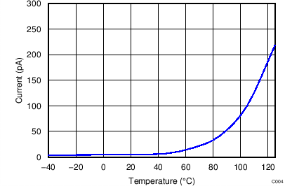
| ILEAK | Leakage current | VIO = 2.5 V | 1 | 10 | nA | |||
| RDYN | Dynamic resistance | DPY package | I/O to GND(2) | 0.8 | Ω | |||
| GND to I/O(2) | 0.7 | |||||||
| DQA package | I/O to GND(2) | 0.96 | ||||||
| GND to I/O(2) | 0.9 | |||||||
| CAPACITANCE | ||||||||
| CL | Line capacitance | VIO = 2.5 V, f = 1 MHz, I/O to GND | TPD1E05U06-Q1 DPY package | 0.42 | pF | |||
| TPD4E05U06-Q1 DQA package | 0.5 | |||||||
| Δ CIO-TO-GND | Variation of input capacitance | GND Pin = 0 V, f = 1 MHz, VBIAS = 2.5 V, Channel x pin to GND – channel y pin to GND |
0.05 | 0.08 | pF | |||
| CCROSS | Channel to channel input capacitance | GND Pin = 0 V, f = 1 MHz, VBIAS = 2.5 V, between channel pins | 0.04 | 0.08 | pF | |||
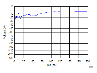
(1) Transition line pulse with 100 ns width, 200 ps rise time.
(2) Extraction of RDYN using least squares fit of TLP characteristics between I = 5 A and I = 10 A.
6.7 Typical Characteristics
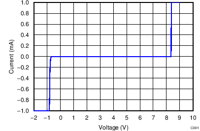
Current vs Voltage DC Voltage Sweep I-V Curve
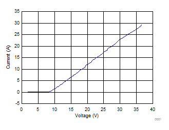
Positive TLP Plot I/O to GND
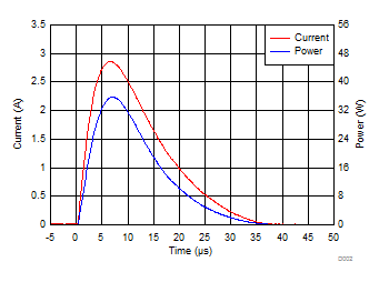
Surge Curve (tp = 8/20 µs), Pin I/O to GND
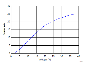
Negative TLP Plot I/O to GND
