SLVSBQ8D December 2012 – October 2023 TPD4E1B06
PRODUCTION DATA
- 1
- 1 Features
- 2 Applications
- 3 Description
- 4 Revision History
- 5 Pin Configuration and Functions
- 6 Specifications
- 7 Detailed Description
- 8 Application and Implementation
- 9 Device and Documentation Support
- 10Mechanical, Packaging, and Orderable Information
Package Options
Mechanical Data (Package|Pins)
Thermal pad, mechanical data (Package|Pins)
- DCK|6
Orderable Information
3 Description
The TPD4E1B06 is a 4-channel bi-directional Electrostatic Discharge (ESD) protection diode array. This device features ultra low leakage current (0.5 nA) for precision analog measurements. The ±12 kV contact and ±15 kV air gap ESD protection exceeds IEC 61000-4-2 level 4 requirements. The TPD4E1B06 device's 0.7 pF line capacitance makes it suitable for precision analog, USB2.0, Ethernet, SATA, LVDS, and 1394 interfaces.
Package Information
| PART NUMBER | PACKAGE(1) | PACKAGE SIZE(2) |
|---|---|---|
| TPD4E1B06 | DCK (SC70, 6) | 2 mm × 2.1 mm |
| DRL (SOT, 6) | 1.6 mm × 1.6 mm |
(1) For all available packages, see the orderable addendum at the end of the data sheet.
(2) The package size (length × width) is a nominal value and includes pins, where applicable.
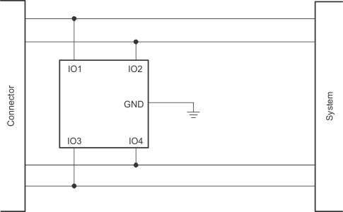
 Simplified Schematic
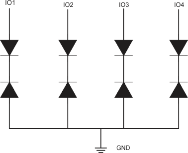
 Functional Block
Diagram