SLVSBQ8D December 2012 – October 2023 TPD4E1B06
PRODUCTION DATA
- 1
- 1 Features
- 2 Applications
- 3 Description
- 4 Revision History
- 5 Pin Configuration and Functions
- 6 Specifications
- 7 Detailed Description
- 8 Application and Implementation
- 9 Device and Documentation Support
- 10Mechanical, Packaging, and Orderable Information
Package Options
Mechanical Data (Package|Pins)
Thermal pad, mechanical data (Package|Pins)
- DCK|6
Orderable Information
8.3.2 Layout Examples
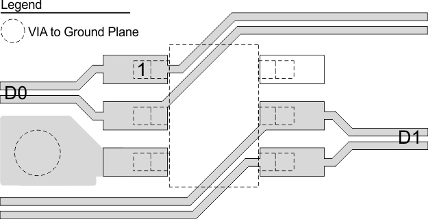
Figure 8-3 shows a layout example for theTPD4E1B06DCK. Pins 1 and 2 and 4 and 5 are routed differentially. Pin 3 is routed to the ground plane. Pin 6 does not have an internal connection in the device and does not need to be routed anywhere on the board. It is also acceptable to connect pin 6 to the ground plane.
 Figure 8-3 DCK Layout Example Showing Two Data Pairs, D0 and D1
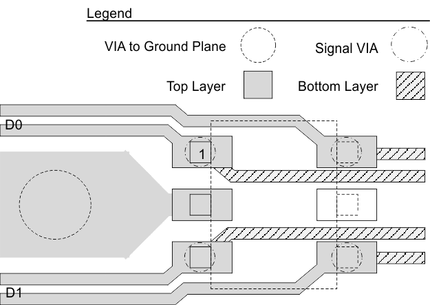
Figure 8-4 shows a layout example for theTPD4E1B06DRL. Pins 1 and 6 and 3 and 4 are routed differentially. Pin 2 is routed to the ground plane. Pin 5 does not have an internal connection in the device and does not need to be routed anywhere on the board. It is also acceptable to connect pin 5 to the ground plane.
 Figure 8-4 DRL Layout Example Showing Two Data Pairs, D0 and D1