SLVSAU0G May 2011 – December 2015 TPD4S014
PRODUCTION DATA.
- 1 Features
- 2 Applications
- 3 Description
- 4 Revision History
- 5 Pin Configuration and Functions
- 6 Specifications
-
7 Detailed Description
- 7.1 Overview
- 7.2 Functional Block Diagram
- 7.3
Feature Description
- 7.3.1 Input Voltage Protection at VBUS up to 28 V DC
- 7.3.2 Low RON nFET Switch
- 7.3.3 ESD Performance D+/D-/ID/VBUS Pins
- 7.3.4 Overvoltage and Undervoltage Lockout Features
- 7.3.5 Capacitance TVS ESD Clamp for USB2.0 Hi-Speed Data Rate
- 7.3.6 Start-up Delay
- 7.3.7 OVP Glitch Immunity
- 7.3.8 Integrated Input Enable and Status Output Signal
- 7.3.9 Thermal Shutdown
- 7.4 Device Functional Modes
- 8 Application and Implementation
- 9 Power Supply Recommendations
- 10Layout
- 11Device and Documentation Support
- 12Mechanical, Packaging, and Orderable Information
Package Options
Mechanical Data (Package|Pins)
- DSQ|10
Thermal pad, mechanical data (Package|Pins)
Orderable Information
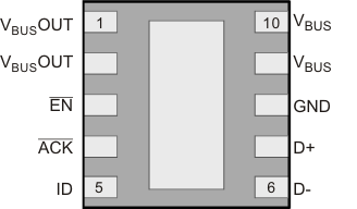
5 Pin Configuration and Functions
DSQ Package
10-Pin WSON
Top Side/See-Through View

Pin Functions
| PIN | TYPE | DESCRIPTION | |
|---|---|---|---|
| NAME | NO. | ||
| VBUSOUT | 1, 2 | Power Output | Connect to PCB internal PCB plane |
| EN | 3 | IO | Enable Active-Low Input. Drive EN low to enable the switch. Drive EN high to disable the switch. |
| ACK | 4 | I | Open-Drain Adapter-Voltage Indicator Output. ACK is driven low after the VIN voltage is stable between UVLO and OVLO for 17 ms (typ). Connect a pullup resistor from ACK to the logic I/O voltage of the host system. |
| ID | 5 | IO | ESD-protected line |
| D– | 6 | IO | ESD-protected line |
| D+ | 7 | IO | ESD-protected line |
| GND | 8 | Ground | Ground |
| VBUS | 9, 10 | USB Input Power | Connector Side of VBUS |
| Central PAD | Central PAD | Heat Sink | Electrically disconnected. Use as heat sink. Connect to GND plane via large PCB PAD |