SLVSAU0G May 2011 – December 2015 TPD4S014
PRODUCTION DATA.
- 1 Features
- 2 Applications
- 3 Description
- 4 Revision History
- 5 Pin Configuration and Functions
- 6 Specifications
-
7 Detailed Description
- 7.1 Overview
- 7.2 Functional Block Diagram
- 7.3
Feature Description
- 7.3.1 Input Voltage Protection at VBUS up to 28 V DC
- 7.3.2 Low RON nFET Switch
- 7.3.3 ESD Performance D+/D-/ID/VBUS Pins
- 7.3.4 Overvoltage and Undervoltage Lockout Features
- 7.3.5 Capacitance TVS ESD Clamp for USB2.0 Hi-Speed Data Rate
- 7.3.6 Start-up Delay
- 7.3.7 OVP Glitch Immunity
- 7.3.8 Integrated Input Enable and Status Output Signal
- 7.3.9 Thermal Shutdown
- 7.4 Device Functional Modes
- 8 Application and Implementation
- 9 Power Supply Recommendations
- 10Layout
- 11Device and Documentation Support
- 12Mechanical, Packaging, and Orderable Information
Package Options
Mechanical Data (Package|Pins)
- DSQ|10
Thermal pad, mechanical data (Package|Pins)
Orderable Information
6 Specifications
6.1 Absolute Maximum Ratings
over operating free-air temperature range (unless otherwise noted)(1)(2)(1) Stresses above these ratings may cause permanent damage. Exposure to absolute maximum conditions for extended periods may degrade device reliability. These are stress ratings only, and functional operation of the device at these or any other conditions beyond those specified is not implied.
(2) The algebraic convention, whereby the most negative value is a minimum and the most positive value is a maximum.
6.2 ESD Ratings
| VALUE | UNIT | ||||
|---|---|---|---|---|---|
| V(ESD) | Electrostatic discharge | Human-body model (HBM), per ANSI/ESDA/JEDEC JS-001(1) | ±2000 | V | |
| Charged-device model (CDM), per JEDEC specification JESD22-C101(2) | ±1000 | ||||
| IEC 61000-4-2 Contact Discharge | D+, D–, ID, VBUS pins | ±1500 | |||
| IEC 61000-4-2 Air-gap Discharge | D+, D–, ID, VBUS pins | ±1500 | |||
(1) JEDEC document JEP155 states that 500-V HBM allows safe manufacturing with a standard ESD control process. Manufacturing with less than 500-V HBM is possible with the necessary precautions. Pins listed as ±2000 V may actually have higher performance.
(2) JEDEC document JEP157 states that 250-V CDM allows safe manufacturing with a standard ESD control process. Manufacturing with less than 250-V CDM is possible with the necessary precautions. Pins listed as ±1000 V may actually have higher performance.
6.3 Recommended Operating Conditions
over operating free-air temperature range (unless otherwise noted)| MIN | NOM | MAX | UNIT | |||
|---|---|---|---|---|---|---|
| TA | Operating free-air temperature | –40 | 85 | °C | ||
| VI | Input voltage | VBUSOUT | –0.1 | 5.5 | V | |
| VBUS | –0.1 | 5.5 | ||||
| EN | –0.1 | 5.5 | ||||
| ACK | –0.1 | 5.5 | ||||
| D+, D-, ID, | –0.1 | 5.5 | ||||
| IVBUS | VBUS continuous current(1) | VBUSOUT | 2.0 | A | ||
| CVBUS | Capacitance on VBUS | VBUS Pin | 10 | µF | ||
| CVBUSOUT | Capacitance on VBUSOUT | VBUSOUT Pin | 10 | µF | ||
| RACK | Pullup resistor on ACK | ACK Pin | 10 | kΩ | ||
(1) IVBUS Max value is dependent on ambient temperature. See Thermal Shutdown section.
6.4 Thermal Information
| THERMAL METRIC(1) | TPD4S014 | UNIT | |
|---|---|---|---|
| DSQ (WSON) | |||
| 8 PINS | |||
| RθJA | Junction-to-ambient thermal resistance | 70.3 | °C/W |
| RθJCtop | Junction-to-case (top) thermal resistance | 46.3 | °C/W |
| RθJB | Junction-to-board thermal resistance | 33.8 | °C/W |
| ψJT | Junction-to-top characterization parameter | 2.9 | °C/W |
| ψJB | Junction-to-board characterization parameter | 33.5 | °C/W |
| RθJCbot | Junction-to-case (bottom) thermal resistance | 16.3 | °C/W |
(1) For more information about traditional and new thermal metrics, see the IC Package Thermal Metrics application report, SPRA953.
6.5 Electrical Characteristics, EN, ACK, D+, D–, ID Pins
over operating free-air temperature range (unless otherwise noted)6.6 Electrical Characteristics OVP Circuits
over operating free-air temperature range (unless otherwise noted)6.7 Supply Current Consumption
over operating free-air temperature range (unless otherwise noted)| PARAMETER | TEST CONDITIONS | MIN | TYP | MAX | UNIT | |
|---|---|---|---|---|---|---|
| IVBUS | VBUS Operating Current Consumption | No load on VBUS_OUT pin, VBUS = 5 V, EN = 0 V |
147.6 | 160 | µA | |
| IVBUS_OFF | VBUS Operating Current Consumption | No load on VBUS_OUT pin, VBUS = 5 V, EN = 5 V |
111.8 | 120 | µA | |
6.8 Thermal Shutdown Feature
over operating free-air temperature range (unless otherwise noted)| PARAMETER | TEST CONDITIONS | MIN | TYP | MAX | UNIT | |
|---|---|---|---|---|---|---|
| TSHDN | Thermal Shutdown | 144 | °C | |||
| TSHDN-HYS | Thermal-Shutdown Hysteresis | 23 | °C | |||
6.9 Typical Characteristics
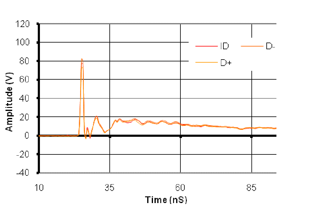
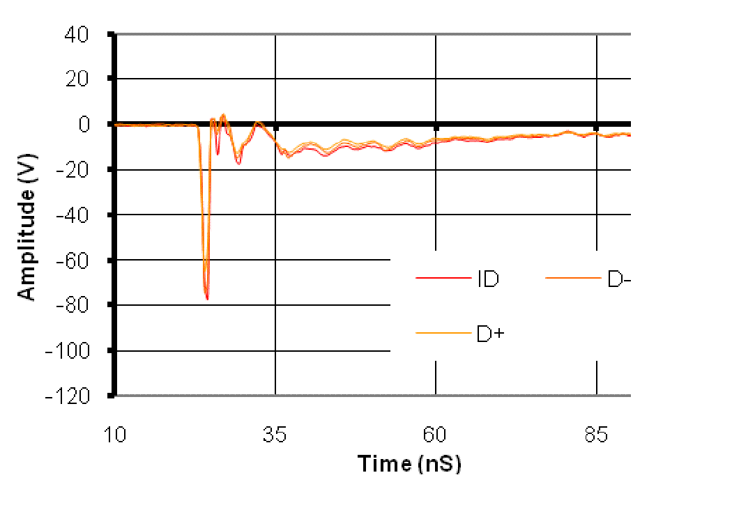 Figure 1. IEC61000-4-2 -8-kV Contact Waveform
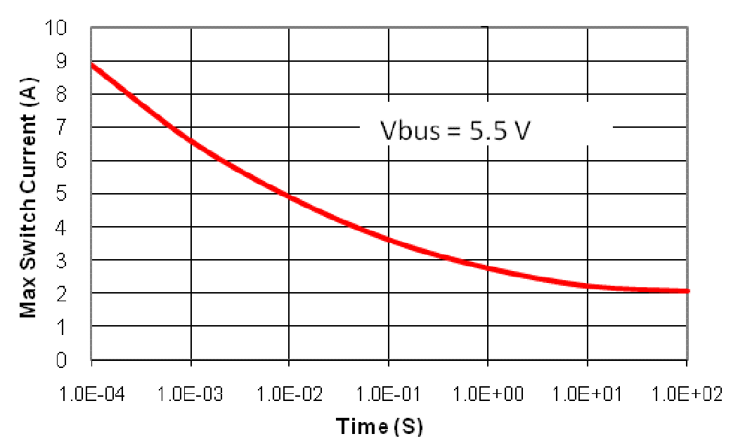
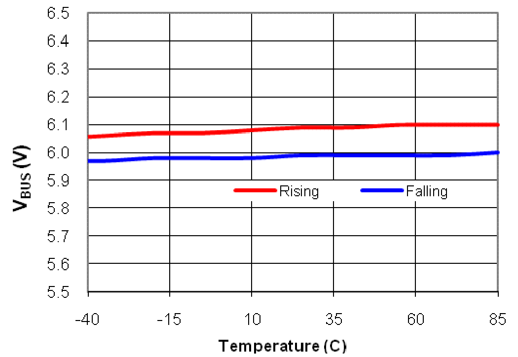
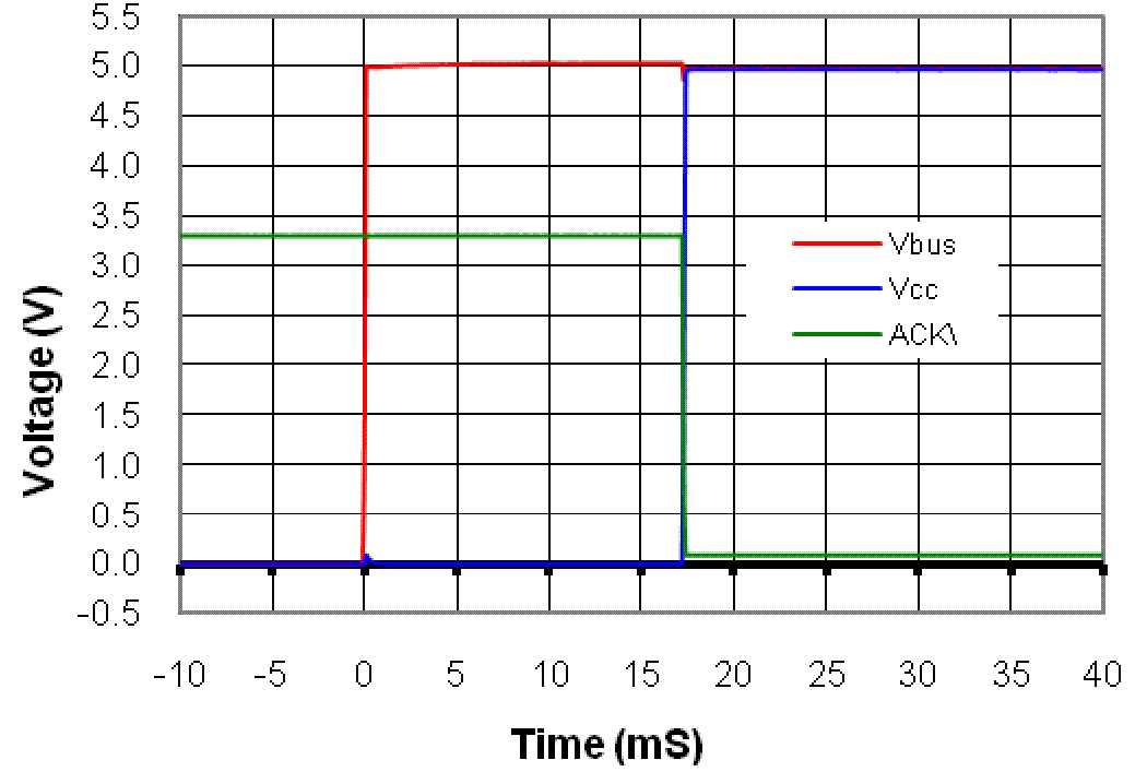
.
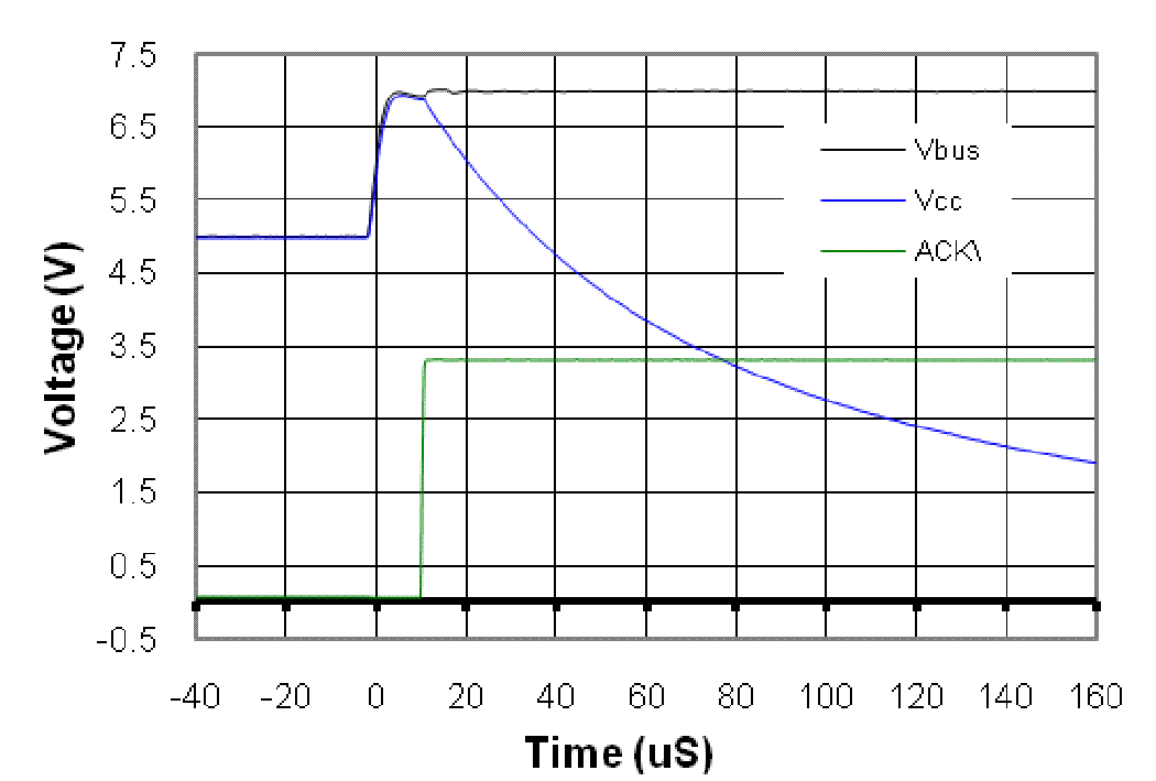
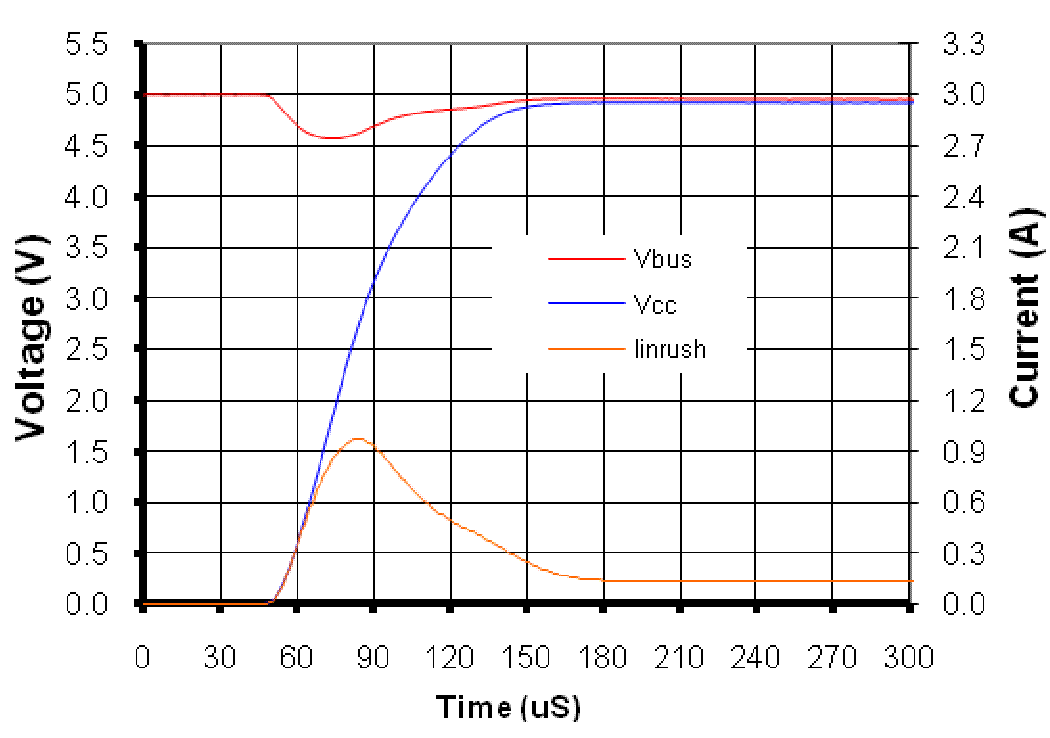
Figure 9. Device Turn on Characteristics
