SLLS876B August   2008  – May 2016 TPD6F002

PRODUCTION DATA.  

  1. Features
  2. Applications
  3. Description
  4. Revision History
  5. Pin Configuration and Functions
  6. Specifications
    1. 6.1 Absolute Maximum Ratings
    2. 6.2 ESD Ratings
    3. 6.3 Recommended Operating Conditions
    4. 6.4 Thermal Information
    5. 6.5 Electrical Characteristics
    6. 6.6 Typical Characteristics
  7. Detailed Description
    1. 7.1 Overview
    2. 7.2 Functional Block Diagram
    3. 7.3 Feature Description
      1. 7.3.1 Six-Channel EMI Filtering
      2. 7.3.2 Pi-Style Filter Configuration
      3. 7.3.3 Robust ESD Protection
      4. 7.3.4 Low Leakage Current
      5. 7.3.5 Space-Saving WSON Package
    4. 7.4 Device Functional Modes
  8. Application and Implementation
    1. 8.1 Application Information
    2. 8.2 Typical Application
      1. 8.2.1 Design Requirements
      2. 8.2.2 Detailed Design Procedure
        1. 8.2.2.1 Signal Range on All Protected Lines
        2. 8.2.2.2 Operating Frequency
        3. 8.2.2.3 Crosstalk Response
      3. 8.2.3 Application Curve
  9. Power Supply Recommendations
  10. 10Layout
    1. 10.1 Layout Guidelines
    2. 10.2 Layout Example
  11. 11Device and Documentation Support
    1. 11.1 Community Resources
    2. 11.2 Trademarks
    3. 11.3 Electrostatic Discharge Caution
    4. 11.4 Glossary
  12. 12Mechanical, Packaging, and Orderable Information

Package Options

Refer to the PDF data sheet for device specific package drawings

Mechanical Data (Package|Pins)
  • DSV|12
Thermal pad, mechanical data (Package|Pins)
Orderable Information

5 Pin Configuration and Functions

DSV Package
12-Pin WSON
Top View
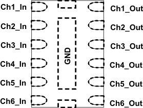
TPD6F002 po_lls876.gif

Pin Functions

PIN TYPE DESCRIPTION
NAME NO.
ChX_In 1, 2, 3, 4, 5, 6 I/O ESD-protected channel, connected to corresponding ChX_Out
ChX_Out 7, 8, 9, 10, 11, 12 I/O ESD-protected channel, connected to corresponding ChX_Inx
GND GND G Ground