SLIS172 December 2015 TPIC2040
PRODUCTION DATA.
- 1 Features
- 2 Applications
- 3 Description
- 4 Revision History
- 5 Description (continued)
- 6 Pin Configuration and Functions
-
7 Specifications
- 7.1 Absolute Maximum Ratings
- 7.2 ESD Ratings
- 7.3 Recommended Operating Conditions
- 7.4 Thermal Information
- 7.5 Electrical Characteristics - Common Part
- 7.6 Electrical Characteristics - Charge Pump
- 7.7 Electrical Characteristics - LDO Pre Driver Part
- 7.8 Electrical Characteristics - Spindle Motor Driver Part
- 7.9 Electrical Characteristics - Sled Motor Driver Part
- 7.10 Electrical Characteristics - Focus/ Tilt/Tracking/Driver Part
- 7.11 Electrical Characteristics - Load Driver Part
- 7.12 Electrical Characteristics - Current Switch Part
- 7.13 Electrical Characteristics - Actuator Protection
- 7.14 Electrical Characteristics - Serial Port Voltage Levels
- 7.15 Serial Port I/F Write Timing Requirements
- 7.16 Serial I/F Read Timing Requirements
- 7.17 Typical Characteristics
-
8 Detailed Description
- 8.1 Overview
- 8.2 Functional Block Diagram
- 8.3 Feature Description
- 8.4 Device Functional Modes
- 8.5 Programming
- 8.6
Register Maps
- 8.6.1 Register State Transition
- 8.6.2 DAC Register (12-Bit Write Only)
- 8.6.3 Control Register
- 8.6.4
Detailed Description of Registers
- 8.6.4.1 REG01 12bit DAC for Tilt (VDAC_MAPSW = 0)
- 8.6.4.2 REG02 12bit DAC for Focus (VDAC_MAPSW = 0)
- 8.6.4.3 REG03 12bit DAC for Tracking (VDAC_MAPSW = 0)
- 8.6.4.4 REG04 10bit DAC for Sled1 (VDAC_MAPSW = 0)
- 8.6.4.5 REG05 10bit DAC for Sled2 (VDAC_MAPSW = 0)
- 8.6.4.6 REG08 12bit DAC for Spindle (VDAC_MAPSW = 0)
- 8.6.4.7 REG09 12bit DAC for Load (VDAC_MAPSW = 0)
- 8.6.4.8 REG6A 8-Bit Control Register for CSW_OCP (REG6A)
- 8.6.4.9 REG6C 8-Bit Control Register for Parm1 (REG6C)
- 8.6.4.10 REG6F 8-Bit Control Register for MonitorSet (REG6F)
- 8.6.4.11 REG70 8-Bit Control Register for DriverEna (REG70)
- 8.6.4.12 REG71 8-Bit Control Register for FuncEna (REG71)
- 8.6.4.13 REG72 8-Bit Control Register for ACTCfg (REG72)
- 8.6.4.14 REG73 8-Bit Control Register for Parm0 (REG73)
- 8.6.4.15 REG74 8-Bit Control Register for OptSet (REG74)
- 8.6.4.16 REG75 8-Bit Control Register for TSD_TUP (REG75)
- 8.6.4.17 REG76 8-Bit Control Register for WriteEna (REG76)
- 8.6.4.18 REG77 8-Bit Control Register for ClrReg (REG77)
- 8.6.4.19 REG78 8-Bit Control Register for ActTemp (REG78)
- 8.6.4.20 REG79 8-Bit Control Register for UVLOMon (REG79)
- 8.6.4.21 REG7A 8-Bit Control Register for TsdMon (REG7A)
- 8.6.4.22 REG7B 8-Bit Control Register for ProtMon (REG7B)
- 8.6.4.23 REG7E 8-Bit Control Register for Version (REG7E)
- 8.6.4.24 REG7F 8-Bit Control Register for Status (REG7F)
-
9 Application and Implementation
- 9.1
Application Information
- 9.1.1 DAC Type
- 9.1.2 Example of 12-Bit DAC Sampling Rate for FCS/TRK/TLT
- 9.1.3 Digital Input Coding
- 9.1.4 Example Timing of Target Control System
- 9.1.5 Spindle Motor Driver Part
- 9.1.6 Sled Driver Part
- 9.1.7 Load Driver Part
- 9.1.8 Focus/Track/Tilt Driver Part
- 9.1.9 9-V LDO
- 9.1.10 Monitor Signal on GPOUT
- 9.2 Typical Application
- 9.1
Application Information
- 10Power Supply Recommendations
- 11Layout
- 12Device and Documentation Support
- 13Mechanical, Packaging, and Orderable Information
Package Options
Mechanical Data (Package|Pins)
- DBT|38
Thermal pad, mechanical data (Package|Pins)
Orderable Information
11 Layout
11.1 Layout Guidelines
- CV3P3V requires an external capacitor. Because these are reference voltage for device, locate the capacitor as close to device as possible. Keep away from noise sources.
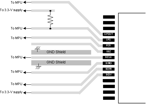
- TI recommends SCLK ground shielding.
- LINFB is feedback pin for LDO. External divided resistors should be located closer to LINFB pin.
11.2 Layout Example
 Figure 60. Layout Recommendation