SLIS172 December 2015 TPIC2040
PRODUCTION DATA.
- 1 Features
- 2 Applications
- 3 Description
- 4 Revision History
- 5 Description (continued)
- 6 Pin Configuration and Functions
-
7 Specifications
- 7.1 Absolute Maximum Ratings
- 7.2 ESD Ratings
- 7.3 Recommended Operating Conditions
- 7.4 Thermal Information
- 7.5 Electrical Characteristics - Common Part
- 7.6 Electrical Characteristics - Charge Pump
- 7.7 Electrical Characteristics - LDO Pre Driver Part
- 7.8 Electrical Characteristics - Spindle Motor Driver Part
- 7.9 Electrical Characteristics - Sled Motor Driver Part
- 7.10 Electrical Characteristics - Focus/ Tilt/Tracking/Driver Part
- 7.11 Electrical Characteristics - Load Driver Part
- 7.12 Electrical Characteristics - Current Switch Part
- 7.13 Electrical Characteristics - Actuator Protection
- 7.14 Electrical Characteristics - Serial Port Voltage Levels
- 7.15 Serial Port I/F Write Timing Requirements
- 7.16 Serial I/F Read Timing Requirements
- 7.17 Typical Characteristics
-
8 Detailed Description
- 8.1 Overview
- 8.2 Functional Block Diagram
- 8.3 Feature Description
- 8.4 Device Functional Modes
- 8.5 Programming
- 8.6
Register Maps
- 8.6.1 Register State Transition
- 8.6.2 DAC Register (12-Bit Write Only)
- 8.6.3 Control Register
- 8.6.4
Detailed Description of Registers
- 8.6.4.1 REG01 12bit DAC for Tilt (VDAC_MAPSW = 0)
- 8.6.4.2 REG02 12bit DAC for Focus (VDAC_MAPSW = 0)
- 8.6.4.3 REG03 12bit DAC for Tracking (VDAC_MAPSW = 0)
- 8.6.4.4 REG04 10bit DAC for Sled1 (VDAC_MAPSW = 0)
- 8.6.4.5 REG05 10bit DAC for Sled2 (VDAC_MAPSW = 0)
- 8.6.4.6 REG08 12bit DAC for Spindle (VDAC_MAPSW = 0)
- 8.6.4.7 REG09 12bit DAC for Load (VDAC_MAPSW = 0)
- 8.6.4.8 REG6A 8-Bit Control Register for CSW_OCP (REG6A)
- 8.6.4.9 REG6C 8-Bit Control Register for Parm1 (REG6C)
- 8.6.4.10 REG6F 8-Bit Control Register for MonitorSet (REG6F)
- 8.6.4.11 REG70 8-Bit Control Register for DriverEna (REG70)
- 8.6.4.12 REG71 8-Bit Control Register for FuncEna (REG71)
- 8.6.4.13 REG72 8-Bit Control Register for ACTCfg (REG72)
- 8.6.4.14 REG73 8-Bit Control Register for Parm0 (REG73)
- 8.6.4.15 REG74 8-Bit Control Register for OptSet (REG74)
- 8.6.4.16 REG75 8-Bit Control Register for TSD_TUP (REG75)
- 8.6.4.17 REG76 8-Bit Control Register for WriteEna (REG76)
- 8.6.4.18 REG77 8-Bit Control Register for ClrReg (REG77)
- 8.6.4.19 REG78 8-Bit Control Register for ActTemp (REG78)
- 8.6.4.20 REG79 8-Bit Control Register for UVLOMon (REG79)
- 8.6.4.21 REG7A 8-Bit Control Register for TsdMon (REG7A)
- 8.6.4.22 REG7B 8-Bit Control Register for ProtMon (REG7B)
- 8.6.4.23 REG7E 8-Bit Control Register for Version (REG7E)
- 8.6.4.24 REG7F 8-Bit Control Register for Status (REG7F)
-
9 Application and Implementation
- 9.1
Application Information
- 9.1.1 DAC Type
- 9.1.2 Example of 12-Bit DAC Sampling Rate for FCS/TRK/TLT
- 9.1.3 Digital Input Coding
- 9.1.4 Example Timing of Target Control System
- 9.1.5 Spindle Motor Driver Part
- 9.1.6 Sled Driver Part
- 9.1.7 Load Driver Part
- 9.1.8 Focus/Track/Tilt Driver Part
- 9.1.9 9-V LDO
- 9.1.10 Monitor Signal on GPOUT
- 9.2 Typical Application
- 9.1
Application Information
- 10Power Supply Recommendations
- 11Layout
- 12Device and Documentation Support
- 13Mechanical, Packaging, and Orderable Information
Package Options
Mechanical Data (Package|Pins)
- DBT|38
Thermal pad, mechanical data (Package|Pins)
Orderable Information
7 Specifications
7.1 Absolute Maximum Ratings
over operating free-air temperature range (unless otherwise noted) (1)| MIN | MAX | UNIT | ||
|---|---|---|---|---|
| + 5 V supply voltage P5V, P5V_SPM | 6 | V | ||
| Spindle output peak voltage | 7 | V | ||
| Input/output voltage | –0.3 | VCC + 0.3 V | V | |
| Spindle output current | 1.0 | A | ||
| Spindle output peak current (PW ≦ 2 ms, Duty ≦ 30%) | 2.5 | A | ||
| Sled output peak current | 0.8 | A | ||
| Focus/tilt/tracking driver output peak current | 1.5 | A | ||
| Load driver output peak current | 0.8 | A | ||
| Power dissipation | See Thermal Information | |||
| Operating temperature | –20 | 75 | °C | |
| Tstg | Storage temperature | –50 | 150 | °C |
(1) Stresses beyond those listed under Absolute Maximum Ratings may cause permanent damage to the device. These are stress ratings only, which do not imply functional operation of the device at these or any other conditions beyond those indicated under Recommended Operating Conditions. Exposure to absolute-maximum-rated conditions for extended periods may affect device reliability.
7.2 ESD Ratings
| VALUE | UNIT | |||
|---|---|---|---|---|
| V(ESD) | Electrostatic discharge | Human-body model (HBM), per ANSI/ESDA/JEDEC JS-001(1) | ±2000 | V |
| Charged-device model (CDM), per JEDEC specification JESD22-C101(2) | ±500 | |||
(1) JEDEC document JEP155 states that 500-V HBM allows safe manufacturing with a standard ESD control process.
(2) JEDEC document JEP157 states that 250-V CDM allows safe manufacturing with a standard ESD control process.
7.3 Recommended Operating Conditions
over operating free-air temperature range (unless otherwise noted)| MIN | NOM | MAX | UNIT | ||
|---|---|---|---|---|---|
| P5V | Operating supply voltage (apply for P5V) | 4.5 | 5.0 | 5.5 | V |
| VSIOV | SIOV voltage | 3.0 | 3.3 | 3.6 | V |
| VSIFH | XMUTE, SIMO, SSZ, SCLK pin H level input voltage range | 2.2 | SIOV + 0.2 | V | |
| VSIFL | XMUTE, SIMO, SSZ, SCLK pin L level input voltage range | –0.2 | 0.8 | V | |
| ISPMOA | Spindle output average current (U, V, W total) | 700 | mA | ||
| ISPMO | Spindle output current | 700 | mA | ||
| ISLDOA | Sled output average current | 400 | mA | ||
| IACTOA | Focus / tracking / tilt / loading output average current | 400 | mA | ||
| ICSWOA | CSWO output average current | 500 | mA | ||
| Fck | SCLK frequency | 30 | 33.8688 | 35 | MHz |
| TO | Operating temperature | –20 | 25 | 75 | °C |
7.4 Thermal Information
| THERMAL METRIC(1) | TPIC2040 | UNIT | |
|---|---|---|---|
| DBT (TSSOP) | |||
| 38 PINS | |||
| RθJA | Junction-to-ambient thermal resistance(2) | 81.2 | °C/W |
| RθJC(top) | Junction-to-case (top) thermal resistance | 27.2 | °C/W |
| RθJB | Junction-to-board thermal resistance | 42.3 | °C/W |
| ψJT | Junction-to-top characterization parameter | 1.7 | °C/W |
| ψJB | Junction-to-board characterization parameter | 41.7 | °C/W |
| RθJC(bot) | Junction-to-case (bottom) thermal resistance | N/A | °C/W |
(1) For more information about traditional and new thermal metrics, see the Semiconductor and IC Package Thermal Metrics application report, SPRA953.
(2) The JEDEC specification low K (1 s) board design used to derive this data.
7.5 Electrical Characteristics – Common Part
over recommended operating free-air temperature range (P5V ≈ 4.5 to 5.5 V, TA ≈ –20℃ to 75℃, unless otherwise noted)| PARAMETER | TEST CONDITIONS | MIN | TYP | MAX | UNIT | |
|---|---|---|---|---|---|---|
| ISTBY | Stand by supply current | LIN3P3_DIS = 1, XSLEEP = L | 1.0 | mA | ||
| VCV3 | CV3P3 output voltage | Iload = 25 mA | 2.97 | 3.3 | 3.63 | V |
| RXM | XMUTE pulldown resistor | 80 | 200 | 320 | kΩ | |
| RXRST | XRESET pullup resistor | 13.2 | 33 | 52.8 | kΩ | |
| VXRSTL | XRESET low level output voltage | SIOV = 3.3 V, IOL = –100 µA | 0.3 | V | ||
| TPOR | Power-on reset delay | 15 | 20 | 25 | ms | |
| RXFG | XFG output resistor | 100 | 200 | 300 | Ω | |
| VXFGH | XFG high-level output voltage | SIOV = 3.3 V, XSLEEP = 1, IOH = 100 µA |
SIOV – 0.3 | V | ||
| VXFGL | XFG low-level output voltage | SIOV = 3.3 V, XSLEEP = 1, IOL = –100 µA |
0.3 | V | ||
| RGPO | GPOUT output resistor | 100 | 200 | 300 | Ω | |
| VGPOH | GPOUT high-level output voltage | SIOV = 3.3 V, XSLEEP = 1, GPOUT_ENA = 1,GPOUT_HL = 1, IOH = 100 µA |
SIOV – 0.3 | V | ||
| VGPOL | GPOUT low-level output voltage | SIOV = 3.3 V, XSLEEP = 1, GPOUT_ENA = 1, GPOUT_HL = 0, IOH = 100 µA |
0.3 | V | ||
| tTSD | Thermal protect on temperature | Design specified value | 135 | 150 | 165 | ºC |
| hytTSD | Thermal protect hysteresis temperature | 5 | 15 | 25 | ºC | |
| Vonvcc | P5V reset on voltage | 3.3 | 3.5 | 3.7 | V | |
| Voffvcc | P5V reset off voltage | 3.5 | 3.7 | 3.9 | V | |
| Vhysvcc | P5V reset voltage hysteresis | 100 | 200 | 300 | mV | |
| VonCV3 | CV3P3 reset on voltage | 2.4 | 2.5 | 2.6 | V | |
| VoffCV3 | CV3P3 reset off voltage | 2.5 | 2.6 | 2.7 | V | |
| VonSIO | SIOV reset on voltage | 2.4 | 2.5 | 2.6 | V | |
| VoffSIO | SIOV reset off voltage | 2.5 | 2.6 | 2.7 | V | |
| VhysSIO | SIOV reset voltage hysteresis | 20 | 100 | 140 | mV | |
| VovpspmOn | OVP detection voltage (spindle) (1) | 5.9 | 6.2 | 6.4 | V | |
| VovpspmOff | OVP release voltage (spindle) (1) | 5.7 | 6.0 | 6.2 | V | |
| VovpSpmHys | OVP voltage hysteresis (spindle) (1) | 50 | 200 | 300 | mV | |
| VovpOn | OVP detection voltage (except spindle)(1) |
6.2 | 6.5 | 6.7 | V | |
| VovpOff | OVP release voltage (except spindle)(1) |
6.0 | 6.3 | 6.5 | V | |
| VovpHys | OVP voltage hysteresis (except spindle)(1) |
50 | 200 | 300 | mV | |
| VonLinF | LINFB reset on voltage | 0.83 | 0.93 | 1.03 | V | |
| VoffLinF | LINFB reset off voltage | 0.88 | 0.98 | 1.08 | V | |
| VhysLINF | LINFB reset voltage hysteresis | 20 | 50 | 80 | mV | |
(1) Those are value as protection functions only, and stress beyond those listed under Recommended Operating Conditions may cause permanent damage to the device.
7.6 Electrical Characteristics – Charge Pump
over recommended operating free-air temperature range (P5V ≈ 4.5 to 5.5 V, TA ≈ –20℃ to 75℃, unless otherwise noted)| PARAMETER | TEST CONDITIONS | MIN | TYP | MAX | UNIT | |
|---|---|---|---|---|---|---|
| FCHGP | Frequency | XSLEEP = 1 | 132.6 | 156 | 179.4 | kHz |
| VCHGP | Output voltage | Ccp1 = Ccp3 = 0.1 µF IO = –1 mA |
7.76 | 9.7 | 11.64 | V |
7.7 Electrical Characteristics – LDO Pre Driver Part
over recommended operating free-air temperature range (P5V ≈ 4.5 to 5.5 V, TA ≈ –20℃ to 75℃, unless otherwise noted)| PARAMETER | TEST CONDITIONS | MIN | TYP | MAX | UNIT | |
|---|---|---|---|---|---|---|
| LINFB_Vth | LINFB threshold voltage | 1.175 | 1.215 | 1.255 | V | |
7.8 Electrical Characteristics – Spindle Motor Driver Part
over recommended operating free-air temperature range (P5V ≈ 4.5 to 5.5 V, TA ≈ –20℃ to 75℃, unless otherwise noted)| PARAMETER | TEST CONDITIONS | MIN | TYP | MAX | UNIT | |
|---|---|---|---|---|---|---|
| RttlSPM | Total output resistance High side + low side(1) |
IOUT = 0.5 A | 0.37 | 0.7 | Ω | |
| ResSPM | Resolution | 12 | bit | |||
| GnSPM | Gain | Magnification to 1.0 input | 5.2 | 6.0 | 6.8 | times |
| WidDZSPM | Spindle dead band | Forward | 12h | 52h | 92h | |
| Reverse | –92h | –52h | –12h | |||
| WidDZSPMLS | Spindle dead band (LS mode) | –40h | 0h | 40h | ||
| SPMClim | Current limit | SPM_RCOM_SEL = 00 | 801 | 890 | 979 | mA |
| SPM_RCOM_SEL = 01 | 882 | 980 | 1078 | mA | ||
| SPM_RCOM_SEL = 10 | 652 | 725 | 798 | mA | ||
| SPM_RCOM_SEL = 11 | 705 | 784 | 863 | mA | ||
(1) IncldRcs
7.9 Electrical Characteristics – Sled Motor Driver Part
over recommended operating free-air temperature range (P5V ≈ 4.5 to 5.5 V, TA ≈ –20℃ to 75℃, unless otherwise noted)| PARAMETER | TEST CONDITIONS | MIN | TYP | MAX | UNIT | |
|---|---|---|---|---|---|---|
| RttlSLD | Total output resistance High side + low side |
IO = 0.5 A | 0.9 | 1.3 | Ω | |
| ResSLD | Resolution | 10 | bit | |||
| WidDZSLD | Input dead band | Forward | 2h | 1Fh | 60h | |
| Reverse | –60h | –1Fh | –2h | |||
| GnSLD | Sled current gain | P5V = 5 V RL = 10 Ω, 2.2 mH VSLED = 7FFh |
380 | 440 | 500 | mA |
| VthEdetSLD | END_DET BEMF threshold voltage | SLEDENDTH<2:0> = 000 | 26 | 46 | 66 | mV |
| SLEDENDTH<2:0> = 010 | 42 | 82 | 122 | mV | ||
| SLEDENDTH<2:0> = 011 | 9 | 22 | 35 | mV | ||
| SLEDENDTH<2:0> = 100 | 65 | 125 | 185 | mV | ||
| SLEDENDTH<2:0> = 101 | 55 | 105 | 155 | mV | ||
| SLEDENDTH<2:0> = 111 | 70 | 145 | 220 | mV | ||
7.10 Electrical Characteristics – Focus/ Tilt/Tracking/Driver Part
over recommended operating free-air temperature range (P5V ≈ 4.5 to 5.5 V, TA ≈ –20℃ to 75℃, unless otherwise noted)| PARAMETER | TEST CONDITIONS | MIN | TYP | MAX | UNIT | |
|---|---|---|---|---|---|---|
| RttlAct | Total output resistance High Side + Low Side (Focus±, Track±, Tilt±) |
IO = 0.5 A | 0.9 | 1.3 | Ω | |
| ResACT | Resolution | 12 | bit | |||
| VOfstACT | Each channel output offset voltage | DAC_code = 000h | –20 | 0 | 20 | mV |
| VOfstDACT | Output offset voltage Focus and Tilt | DIFF_TLT = 1 | –50 | 0 | 50 | mV |
| GnDAct | Difference gain Focus and Tilt | DIFF_TLT = 1 | –1 | 0 | 1 | db |
| GnAct | Gain | Magnification to 1.0 input | 5.2 | 6 | 6.8 | times |
7.11 Electrical Characteristics – Load Driver Part
over recommended operating free-air temperature range (P5V ≈ 4.5 to 5.5 V, TA ≈ –20℃ to 75℃, unless otherwise noted)| PARAMETER | TEST CONDITIONS | MIN | TYP | MAX | UNIT | |
|---|---|---|---|---|---|---|
| RttlLOD | Total output resistance High side + low side (Load±) |
IO = 0.5 A | 0.9 | 1.3 | Ω | |
| ResLOD | Resolution | 12 | bit | |||
| GnLOD | Gain | Magnification to 1.0 input | 5.2 | 6 | 6.8 | times |
| WidDZLOD | Dead band | Forward | 1Fh | |||
| Reverse | –20h | |||||
| TocpLOD | Output 100% limit time | LOAD_05CH = 0 | 0.64 | 0.8 | 0.96 | s |
| IocpLOD | Overcurrent protective level | LOAD_05CH = 1 at Load_OCP_IUP = 0 | 120 | 240 | 400 | mA |
| LOAD_05CH = 1 at Load_OCP_IUP = 1 | 215 | 430 | 645 | mA | ||
| DlyocpLOD | Overcurrent protection delay time | LOAD_05CH = 1 | 0.64 | 0.8 | 0.96 | s |
7.12 Electrical Characteristics – Current Switch Part
over recommended operating free-air temperature range (P5V ≈ 4.5 to 5.5 V, TA ≈ –20℃ to 75℃, unless otherwise noted)| PARAMETER | TEST CONDITIONS | MIN | TYP | MAX | UNIT | |
|---|---|---|---|---|---|---|
| RdsCSW | Rds(on) | IO = 0.2 A | 200 | 500 | mΩ | |
| IlmtCSW | Current limit threshold level | CSW_OCP = 0 | 0.25 | 0.5 | 0.75 | A |
| CSW_OCP = 1 | 0.375 | 0.75 | 1.125 | A | ||
| CSW_OCP = 2 | 0.5 | 1.0 | 1.5 | A | ||
| ThlCSW | Protection hold time | 1.47 | 1.6 | 2.0 | ms | |
7.13 Electrical Characteristics – Actuator Protection
over recommended operating free-air temperature range (P5V ≈ 4.5 to 5.5 V, TA ≈ –20℃ to 75℃, unless otherwise noted)| PARAMETER | TEST CONDITIONS | MIN | TYP | MAX | UNIT | |
|---|---|---|---|---|---|---|
| TintACTTEMP | Update cycle | 21 | 26 | 31 | ms | |
7.14 Electrical Characteristics – Serial Port Voltage Levels
over recommended operating free-air temperature range (P5V ≈ 4.5 to 5.5 V, TA ≈ –20℃ to 75℃, unless otherwise noted)| PARAMETER | TEST CONDITIONS | MIN | TYP | MAX | UNIT | |
|---|---|---|---|---|---|---|
| SOMI | High-level output voltage, VOH | IOH = 1 mA | 80 % SIOV |
V | ||
| SOMI | Low-level output voltage, VOL | IOL = 1 mA | 20% SIOV |
V | ||
| SIMO | High-level input voltage, VIH | 70% SIOV |
V | |||
| SIMO | Low level input voltage, VIL | 20% SIOV |
V | |||
| SIMO | Input rise/fall time | 10% 90% SIOV | 3.5 | ns | ||
| SOMI | Output rise/fall time(1) | Cload = 30 pF, 10% 90% SIOV | 10 | ns | ||
| SCLK | Internal pulldown resistance | 80 | 200 | 320 | kΩ | |
| SIMO | 80 | 200 | 320 | kΩ | ||
| SSZ | Internal pullup resistance | 80 | 200 | 320 | kΩ | |
(1) Specified by design
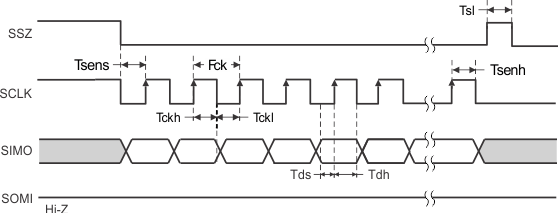
7.15 Serial Port I/F Write Timing Requirements
see (1)| MIN | NOM | MAX | UNIT | |||
|---|---|---|---|---|---|---|
| Fck | SCLK clock frequency | SIOV = 3.3 V | 35 | MHz | ||
| tckl | SCLK low time | 11 | ns | |||
| tckh | SCLK high time | 11 | ns | |||
| tsens | SSZ setup time | 7 | ns | |||
| tsenh | SSZ hold time | 7 | ns | |||
| tsl | SSZ disable high time | 11 | ns | |||
| tds | SIMO setup time (Write) | 7 | ns | |||
| tdh | SIMO hold time (Write) | 7 | ns | |||
(1) Specified by design
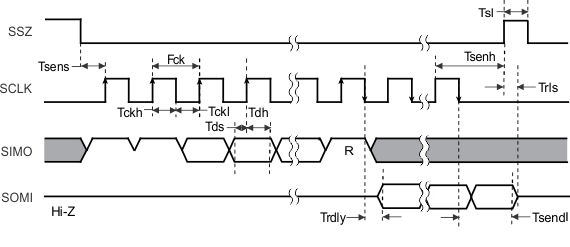
7.16 Serial I/F Read Timing Requirements
| MIN | NOM | MAX | UNIT | |||
|---|---|---|---|---|---|---|
| Fck | SCLK clock frequency | SIOV = 3.3 V | 35 | MHz | ||
| tckl | SCLK low time | 11 | ns | |||
| tckh | SCLK high time | 11 | ns | |||
| tsens | SSZ setup time | 7 | ns | |||
| tsenh | SSZ hold time | 7 | ns | |||
| tsl | SSZ disable high time | 11 | ns | |||
| tds | SIMO setup time (Write) | 7 | ns | |||
| tdh | SIMO hold time (Write) | 7 | ns | |||
| trdly | SOMI delay time (Read) | CLOAD = 10 pF, SIOV = 3.3 V | 2 | 9 | ns | |
| tsendl | SOMI hold time (Read) | CLOAD = 10 pF, SIOV = 3.3 V | 2 | 9 | ns | |
| trls | SOMI release time (Read) | CLOAD = 10 pF, SIOV = 3.3 V From SSZ rise to SOMI HIZ |
0 | 9 | ns | |
 Figure 1. Serial Port Write Timing
 Figure 2. Serial Port Read Timings
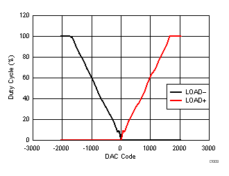
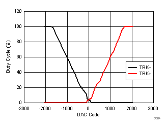
7.17 Typical Characteristics

