SNAS679 September   2016 TPL5010-Q1

PRODUCTION DATA.  

  1. Features
  2. Applications
  3. Description
  4. Revision History
  5. Device Comparison Table
  6. Pin Configuration and Functions
  7. Specifications
    1. 7.1 Absolute Maximum Ratings
    2. 7.2 ESD Ratings
    3. 7.3 Recommended Operating Conditions
    4. 7.4 Thermal Information
    5. 7.5 Electrical Characteristics
    6. 7.6 Timing Requirements
    7. 7.7 Typical Characteristics
  8. Detailed Description
    1. 8.1 Overview
    2. 8.2 Functional Block Diagram
    3. 8.3 Feature Description
      1. 8.3.1 WAKE
      2. 8.3.2 DONE
      3. 8.3.3 RSTn
    4. 8.4 Device Functional Modes
      1. 8.4.1 Startup
      2. 8.4.2 Normal Operating Mode
    5. 8.5 Programming
      1. 8.5.1 Configuring the WAKE Interval with the DELAY/M_RST Pin
      2. 8.5.2 Manual Reset
        1. 8.5.2.1 DELAY/M_RST
        2. 8.5.2.2 Circuitry
      3. 8.5.3 Timer Interval Selection Using External Resistance
      4. 8.5.4 Quantization Error
      5. 8.5.5 Error Due to Real External Resistance
  9. Application and Implementation
    1. 9.1 Application Information
    2. 9.2 Typical Application
      1. 9.2.1 Design Requirements
      2. 9.2.2 Detailed Design Procedure
      3. 9.2.3 Application Curves
  10. 10Power Supply Recommendations
  11. 11Layout
    1. 11.1 Layout Guidelines
    2. 11.2 Layout Example
  12. 12Device and Documentation Support
    1. 12.1 Receiving Notification of Documentation Updates
    2. 12.2 Community Resources
    3. 12.3 Trademarks
    4. 12.4 Electrostatic Discharge Caution
    5. 12.5 Glossary
  13. 13Mechanical, Packaging, and Orderable Information

Package Options

Mechanical Data (Package|Pins)
Thermal pad, mechanical data (Package|Pins)
Orderable Information

11 Layout

11.1 Layout Guidelines

The DELAY/M_RST pin is sensitive to parasitic capacitance. It is suggested that the traces connecting the resistance on this pin to GROUND be kept as short as possible to minimize parasitic capacitance. This capacitance can affect the initial set up of the time interval. Signal integrity on the WAKE and RSTn pins is also improved by keeping the trace length between the TPL5010-Q1 and the µC short to reduce the parasitic capacitance.

11.2 Layout Example
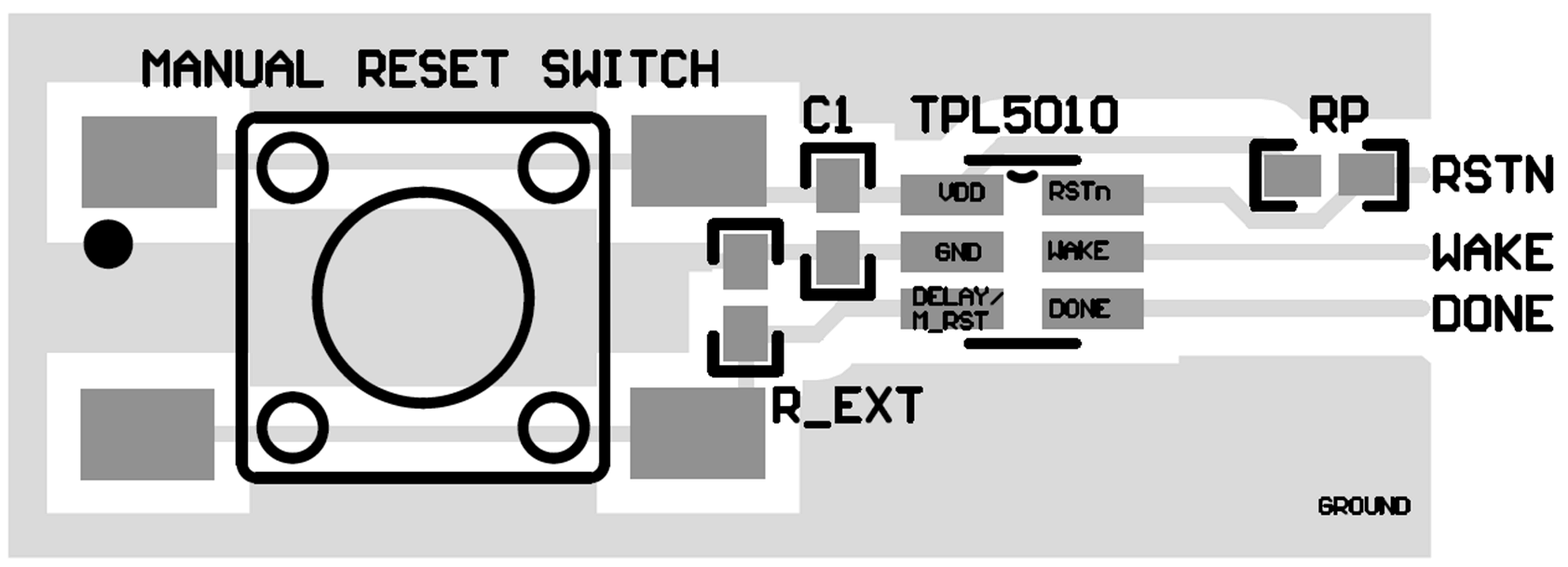
TPL5010-Q1 TPL5010_LAYOUT_REV2.gif Figure 15. Layout