SNAS629C JULY 2013 – December 2014 TPL5100
PRODUCTION DATA.
- 1 Features
- 2 Applications
- 3 Description
- 4 Revision History
- 5 Pin Configuration and Functions
- 6 Specifications
- 7 Detailed Description
- 8 Application and Implementation
- 9 Power Supply Recommendations
- 10Layout
- 11Device and Documentation Support
- 12Mechanical, Packaging, and Orderable Information
Package Options
Mechanical Data (Package|Pins)
- DGS|10
Thermal pad, mechanical data (Package|Pins)
Orderable Information
7 Detailed Description
7.1 Overview
The TPL5100 is a long-term timer for low-power applications. The TPL5100 is designed for use in power cycled applications and provides selectable timing from 16 s to 1024 s. An additional feature is interfacing which is achieved through the TPL5100 to a power-management IC.
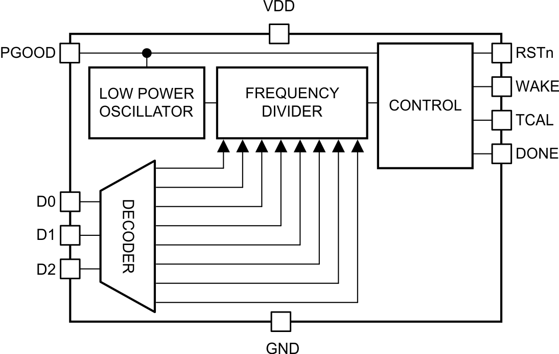
7.2 Functional Block Diagram
7.3 Feature Description
7.3.1 Supervisor Feature
A critical event that can corrupt the memory of a microcontroller is a voltage supply drop (supply lower than minimum operating range), and a reset of the microcontroller is mandatory if this occurs. Since the TPL5100 is the right choice in systems which stay most of the time in deep sleep or completely OFF, due to its ultra-low power consumption, it is fundamental that it takes into account the voltage drop events. The TPL5100 implements the supervisor feature when working with some power-management ICs, which indicate the status of the supply voltage with a power-good or battery-good output. The supervisory functionality is enabled by simply connecting the Battery management power-good output to the TPL5100 PGOOD pin. If this feature is not used connect the PGOOD pin to VDD.
In case the power-management IC detects a voltage drop while the microcontroller is OFF, consequently lowering the PGOOD line, the TPL5100 resets its internal counter and does not allow the micro to turn ON until the PGOOD is high again. This series of events allows the microcontroller to avoid working in an unsafe voltage supply condition. If the PGOOD signal is lowered while the microcontroller is ON, the TPL51000 turns the microcontroller OFF. The micro will be turned ON when PGOOD is high again and the selected delay is elapsed.
7.3.2 Calibration Pulse
The TPL5100 is based on an ultra-low power oscillator, which has a relatively low frequency and low accuracy; however, it shows very good cycle-to-cycle repeatability and very low temperature drift. In most of the applications, the accuracy of the oscillator is enough, but if a more accurate measure of the delay period is required, it is possible to measure the base period of the internal oscillator. A single pulse, which has the same duration as the base period of the internal oscillator, is present at the TCAL pin of the TPL5100. This pulse starts after a half period of the internal oscillator, from the falling edge of the MOS_DRV pulse.
A microcontroller-connected to the TPL5100 can routinely measure the width of the TCAL pulse, using a counter and an external crystal. Once the base period of the TPL5100 is measured, the actual time delay is calculated by multiplying the measured period by a factor, N (see Table 1), dependent upon the nominal selected time delay.
The resolution and the accuracy of the measurement depend upon the external crystal. Since the frequency of the internal oscillator of the TPL5100 is very stable, the measurement of the calibration pulse is suggested only when a high gradient of ambient temperature is observed. The measurement of the TCAL pulse is useful in battery-powered applications that implement a precise battery life counter in the microcontroller.
7.3.2.1 Overview of the Timing Signals MOS_DRV, TCAL, and DONE
Figure 6 shows the timing of PGOOD, MOS_DRV, and TCAL with respect to DONE. The frame, A, shows a typical sequence after the PGOOD, low to high, transition. As soon as PGOOD is high, the internal oscillator is powered ON. At the end of the delay period (tDP), a MOS enable signal (MOS_DRV), followed by a calibration pulse, TCAL, is sent out. The calibration pulse starts after a half period of the internal oscillator from the falling edge of the MOS_DRV signal, and lasts one internal oscillator period. A "DONE" signal is received before the end of the MOS_DRV pulse. As soon as the TPL5100 receives the DONE signal, the counter resets and MOS_DRV and TCAL return to default conditions (MOS_DRV signal high and TCAL signal low).
The frame, B, shows a non-standard sequence. A "DONE" signal has not been received before the end of the MOS_DRV pulse. The MOS_DRV signal stays low for 2 internal oscillator periods. The calibration pulse starts after a half period of the internal oscillator from the falling edge of the MOS_DRV signal, and lasts one internal oscillator period. The external power gating MOS stays ON for 2 internal oscillator periods.
The frame, C, shows a standard sequence, but in this case, the TPL5100 receives the DONE signal when MOS_DRV is high and TCAL pulse is still high. As soon as the TPL5100 recognizes the DONE signal, the counter resets and MOS_DRV and TCAL return to default conditions (MOS_DRV signal high and TCAL signal low).The external power-gating MOS stays ON for the execution time of the program of the connected microcontroller.
The frame, D, shows a typical PGOOD, high to low transition. As soon as PGOOD is low, the internal oscillator is powered OFF and the digital output pins, TCAL and MOS_DRV, are asynchronously reset by the falling edge of the PGOOD signal, such that TCAL resets at low logical values, while MOS_DRV resets at a high logical value. The external power gating MOS stays ON less than the execution time of the program of the connected microcontroller.
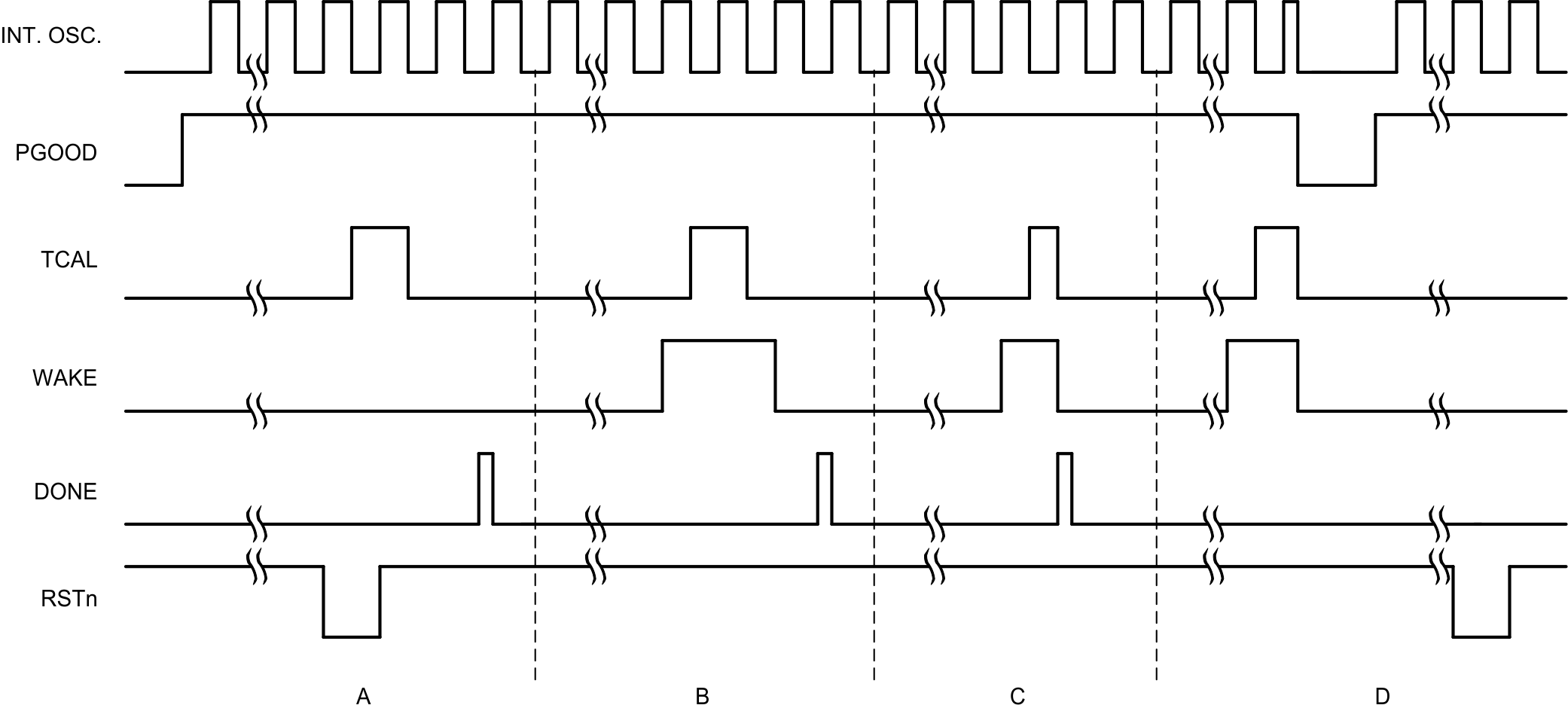 Figure 6. Timing MOS_DRV, TCAL
7.3.3 Configuration and Interface
The time interval between 2 adjacent pulses is selectable through 3 digital input pins (D0, D1, D2) that can be strapped to either VDD (1) or GND (0). Eight possible time delays can be selected, as shown in Table 1.
Table 1. Timer Delay Period
| D2 | D1 | D0 | Time (s) | Factor N |
|---|---|---|---|---|
| 0 | 0 | 0 | 16 | 210 |
| 0 | 0 | 1 | 32 | 211 |
| 0 | 1 | 0 | 64 | 212 |
| 0 | 1 | 1 | 100 | 100*26 |
| 1 | 0 | 0 | 128 | 213 |
| 1 | 0 | 1 | 256 | 214 |
| 1 | 1 | 0 | 512 | 215 |
| 1 | 1 | 1 | 1024 | 216 |
7.4 Device Functional Modes
The TPL5100 is a long-term timer with a watchdog feature for low-power applications. The TPL5100 is designed for use in interrupt-driven applications and provides selectable timing from 1 s to 64 s. An additional supervisor feature is achieved through interfacing the TPL5100 to a power-management IC.