SNAS681A February 2017 – September 2021 TPL5110-Q1
PRODUCTION DATA
- 1 Features
- 2 Applications
- 3 Description
- 4 Revision History
- 5 Pin Configuration and Functions
- 6 Specifications
- 7 Detailed Description
- 8 Application and Implementation
- 9 Power Supply Recommendations
- 10Layout
- 11Device and Documentation Support
- 12Mechanical, Packaging, and Orderable Information
Package Options
Mechanical Data (Package|Pins)
- DDC|6
Thermal pad, mechanical data (Package|Pins)
Orderable Information
7.5.4 Quantization Error
The TPL5110-Q1 can generate 1650 discrete timer intervals in the range of 100ms to 7200s. The first 9 intervals are multiples of 100ms. The remaining 1641 intervals cover the range between 1s to 7200s. Because they are discrete intervals, there is a quantization error associated with each value.
The quantization error can be evaluated according to the following formula:
Equation 3. 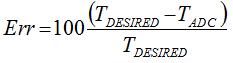
Where:
Equation 4. 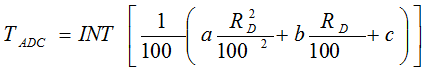
Equation 5. 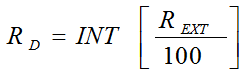
REXT is the resistance calculated with Equation 1 and a,b,c are the coefficients of the equation listed in Table 7-1.