SNAS681A February 2017 – September 2021 TPL5110-Q1
PRODUCTION DATA
- 1 Features
- 2 Applications
- 3 Description
- 4 Revision History
- 5 Pin Configuration and Functions
- 6 Specifications
- 7 Detailed Description
- 8 Application and Implementation
- 9 Power Supply Recommendations
- 10Layout
- 11Device and Documentation Support
- 12Mechanical, Packaging, and Orderable Information
Package Options
Mechanical Data (Package|Pins)
- DDC|6
Thermal pad, mechanical data (Package|Pins)
Orderable Information
7.5.5 Error Due to Real External Resistance
REXT is a theoretical value and may not be available in standard commercial resistor values. It is possible to closely approach the theoretical REXT using two or more standard values in parallel. However, standard values are characterized by a certain tolerance. This tolerance will affect the accuracy of the time interval.
The accuracy can be evaluated using the following procedure:
- Evaluate the min and max values of REXT (REXT_MIN, REXT_MAX with Equation 1 using the selected commercial resistance values and their tolerances.
- Evaluate the time intervals (TADC_MIN[REXT_MIN], TADC_MAX[REXT_MAX]) with Equation 4.
- Find the errors using Equation 3 with TADC_MIN, TADC_MAX.
The example below illustrates the procedure.
- Desired time interval , T_desired = 600s,
- Required REXT, from Equation 1, REXT= 57.44kΩ.
From Table 7-3, REXT can be built with a parallel combination of two commercial values with 1% tolerance: R1=107kΩ, R2=124kΩ. The uncertainty of the equivalent parallel resistance can be found using:
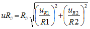
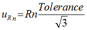
Where uRn (n=1,2) represent the uncertainty of a resistance,
The uncertainty of the parallel resistance is 0.82%, meaning the value of REXT may range between REXT_MIN = 56.96 kΩ and REXT_MAX = 57.90 kΩ.
Using these value of REXT, the digitized timer intervals calculated with Equation 4 are respectively TADC_MIN = 586.85 s and TADC_MAX = 611.3 s, giving an error range of -1.88% / +2.19%. The asymmetry of the error range is due to the quadratic transfer function of the resistance digitizer.