SLVSGL6A July 2022 – December 2022 TPS1HC30-Q1
PRODUCTION DATA
- 1 Features
- 2 Applications
- 3 Description
- 4 Revision History
- 5 Pin Configuration and Functions
- 6 Specifications
- 7 Parameter Measurement Information
-
8 Detailed Description
- 8.1 Overview
- 8.2 Functional Block Diagram
- 8.3
Feature Description
- 8.3.1 Accurate Current Sense
- 8.3.2 Programmable Current Limit
- 8.3.3 Inductive-Load Switching-Off Clamp
- 8.3.4
Full Protections and Diagnostics
- 8.3.4.1 Short-Circuit and Overload Protection
- 8.3.4.2 Open-Load and Short-to-Battery Detection
- 8.3.4.3 Short-to-Battery Detection
- 8.3.4.4 Reverse-Polarity and Battery Protection
- 8.3.4.5 Latch-Off Mode
- 8.3.4.6 Thermal Protection Behavior
- 8.3.4.7 UVLO Protection
- 8.3.4.8 Loss of GND Protection
- 8.3.4.9 Loss of Power Supply Protection
- 8.3.4.10 Reverse Current Protection
- 8.3.4.11 Protection for MCU I/Os
- 8.3.5 Diagnostic Enable Function
- 8.4 Device Functional Modes
- 9 Application and Implementation
- 10Device and Documentation Support
- 11Mechanical, Packaging, and Orderable Information
Package Options
Mechanical Data (Package|Pins)
- PWP|14
Thermal pad, mechanical data (Package|Pins)
- PWP|14
Orderable Information
6.8 Typical Characteristics
All the following data are based on the mean value of the three lots samples, VVBB = 13.5 V if not specified.
| VOUT = 0 V | VEN = 0 V | VDIAG_EN = 0 V |
| VBB Varied |
| IOUT = 0 A | VEN = 0 V | VDIAG_EN = 5 V |
| VBB Varied |
| IOUT = 1 A | VEN = 5 V | VDIAG_EN = 5 V |
| VBB Varied |
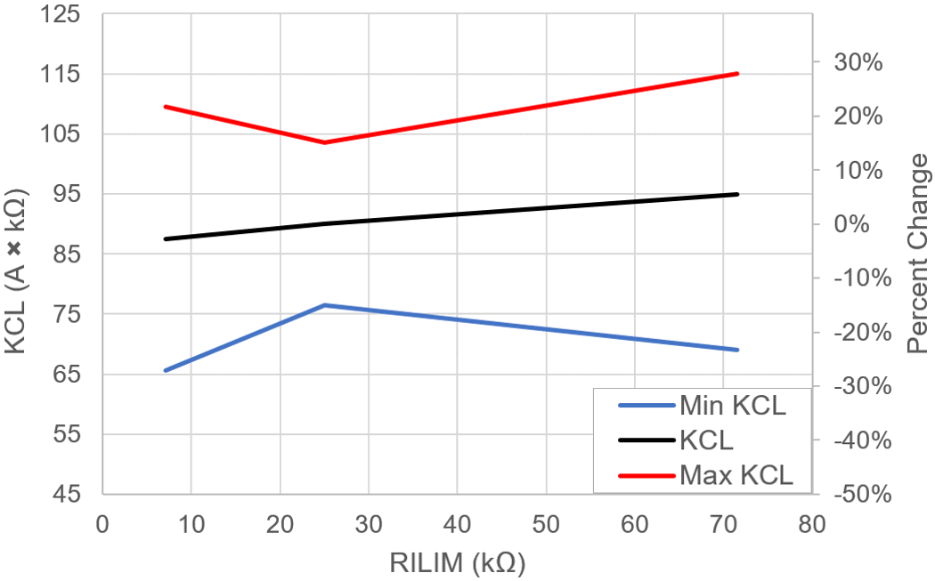
| ROUT = 5 μH and 100 mΩ | VEN = 5 V | VDIAG_EN = 5 V |
| VDS = 3 V |
| IOUT = 1.5 A | VEN = 5 V | VDIAG_EN = 5 V |
| VBB varied | RSNS = 1 kΩ |
| ROUT = 5 μH and 100 mΩ | VEN = 5 V | VDIAG_EN = 5 V |
| VBB varied | RSNS = 1 kΩ |
| ROUT = 10 Ω | VEN = 5 V | VDIAG_EN = 5 V |
| VBB varied | RSNS = 1 kΩ |
| ROUT = 10 Ω | VEN = 5 V | VDIAG_EN = 5 V |
| VBB varied | RSNS = 1 kΩ |
| ROUT = 1 kΩ | VEN = 3.3 to 0 V | VDIAG_EN = 3.3 to 0 V |
| VBB varied | RSNS = 1 kΩ |
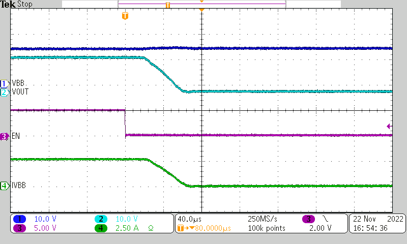
| ROUT = 10 Ω | VEN = 5 to 0 V | VDIAG_EN = 0 V |
| VBB = 13.5 V | RSNS = 1 kΩ |
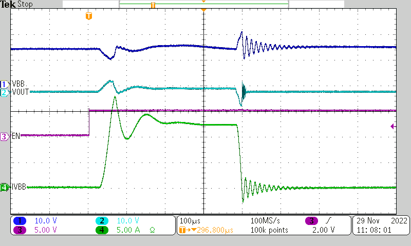
| ROUT = 5 μH and 100 mΩ | VEN = 5 V | VDIAG_EN = 5 V |
| VBB = 13.5 V | RSNS = 1 kΩ | RILIM = 7.15 kΩ |
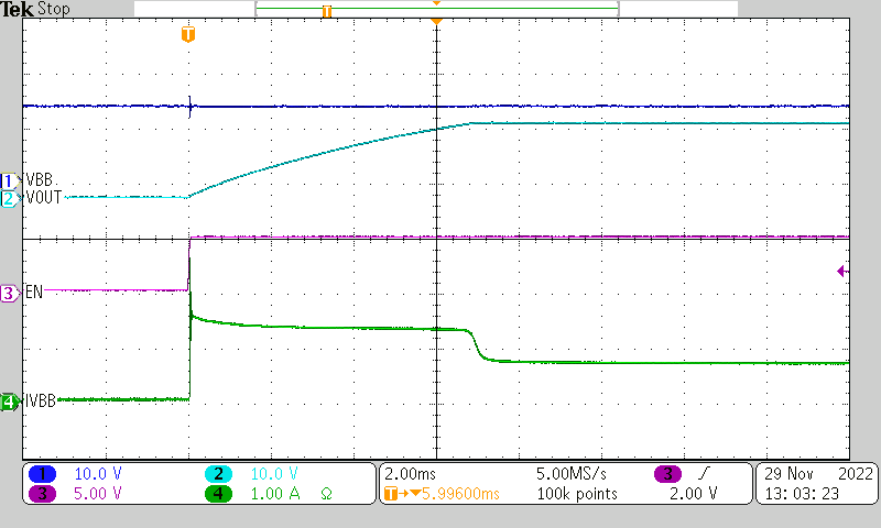
| ROUT = 470 μF and 20 Ω | VEN = 5 V | VDIAG_EN = 5 V |
| VBB = 13.5 V | RSNS = 1 kΩ | RILIM = 71.5 kΩ |
| VOUT = 0 V | VEN = 0 V | VDIAG_EN = 0 V |
| VBB Varied |
| IOUT = 0 A | VEN = 5 V | VDIAG_EN = 5 V |
| VBB Varied |
| IOUT = 1 A | VEN = 5 V | VDIAG_EN = 5 V |
| VBB Varied |
| IOUT = 1 A | VEN = 5 V | VDIAG_EN = 5 V |
| VBB Varied |
| ROUT varied | VEN = 5 V | VDIAG_EN = 5 V |
| VBB = 13.5 V | RSNS = 1 kΩ |
| ROUT = 5 μH and 100 mΩ | VEN = 5 V | VDIAG_EN = 5 V |
| VBB varied | RSNS = 1 kΩ |
| ROUT = 10 Ω | VEN = 5 V | VDIAG_EN = 5 V |
| VBB varied | RSNS = 1 kΩ |
| ROUT = 10 Ω | VEN = 5 V | VDIAG_EN = 5 V |
| VBB varied | RSNS = 1 kΩ |
| ROUT = 1 kΩ | VEN = 0 to 3.3 V | VDIAG_EN = 0 to 3.3 V |
| VBB varied | RSNS = 1 kΩ |
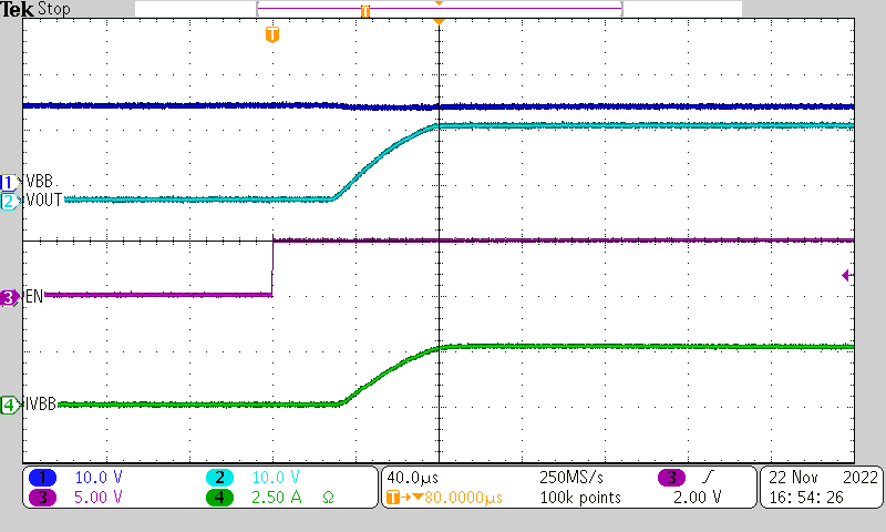
| ROUT = 10 Ω | VEN = 0 to 5 V | VDIAG_EN = 0 V |
| VBB = 13.5 V | RSNS = 1 kΩ |
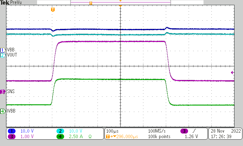
| IOUT = 1 A to 5 A | VEN = 5 V | VDIAG_EN = 5 V |
| VBB = 13.5 V | RSNS = 1 kΩ |
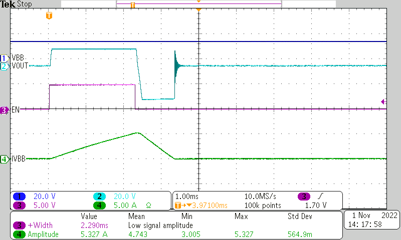
| ROUT = 5 mH | VEN = 5 V | VDIAG_EN = 5 V |
| VBB = 13.5 V | RSNS = 1 kΩ | RILIM = GND |