SLVSD04 April 2015 TPS22860
PRODUCTION DATA.
- 1 Features
- 2 Applications
- 3 Description
- 4 Revision History
- 5 Pin Configuration and Functions
- 6 Specifications
- 7 Detailed Description
- 8 Application and Implementation
- 9 Power Supply Recommendations
- 10Layout
- 11Mechanical, Packaging, and Orderable Information
Package Options
Mechanical Data (Package|Pins)
- DBV|6
Thermal pad, mechanical data (Package|Pins)
Orderable Information
8 Application and Implementation
NOTE
Information in the following applications sections is not part of the TI component specification, and TI does not warrant its accuracy or completeness. TI’s customers are responsible for determining suitability of components for their purposes. Customers should validate and test their design implementation to confirm system functionality.
8.1 Application Information
This section will highlight some of the design considerations when implementing this device in a common application.
8.2 Typical Application
The TPS22860 IC is a high side load switch. The TPS22860 internal components are rated for 1.65-V to 5.5-V supply and support up to 200 mA of load current. The TPS22860 can be used in a variety of applications. Figure 8 below shows a general application of TPS22860 to control the load inrush current.
 Figure 8. Standard Load Switching Application
8.2.1 Design Requirements
Table 2. Component Table
| COMPONENT | DESCRIPTION |
|---|---|
| CIN | Input capacitance(1) |
| LOAD | Load resistance and capacitance will affect the output rise time |
8.2.2 Detailed Design Procedure
8.2.2.1 Inrush Current
To limit the voltage drop on the input supply caused by transient inrush currents when the switch turns on into a discharged load capacitor, a capacitor must be placed between VIN and GND. A 1-µF ceramic capacitor, CIN, placed close to the pins, is usually sufficient. Higher values of CIN can be used to further reduce the voltage drop during high-current applications. When switching heavy loads, TI recommends to have an input capacitor about 10× higher than the output capacitor to avoid excessive voltage drop. Do not float the ON pin.
8.2.2.2 ON/OFF Interface
The load switch is controlled by the voltage at the ON pin. To turn ON, the input voltage must be larger than VIH and to turn off the voltage must be below VIL.
In applications where an ON/OFF signal is not available, connect ON pin to VIN. The TPS22860 will turn ON/OFF in sync with the input supply connected to VIN.
NOTE
Connect a pull down resistor from the ON pin to GND when the ON/OFF signal is driven by a high-impedance (tri-state) driver.
8.2.3 Application Curves
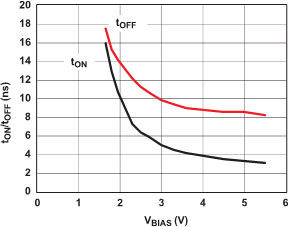
 Figure 9. tON and tOFF vs VBIAS
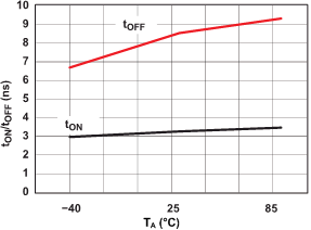
 Figure 10. tON and tOFF vs Temperature (VBIAS = 5 V)