SLVS827D February 2009 – June 2015 TPS22904
PRODUCTION DATA.
- 1 Features
- 2 Applications
- 3 Description
- 4 Revision History
- 5 Device Comparison Table
- 6 Pin Configuration and Functions
- 7 Specifications
- 8 Parameter Measurement Information
- 9 Detailed Description
- 10Application and Implementation
- 11Power Supply Recommendations
- 12Layout
- 13Device and Documentation Support
- 14Mechanical, Packaging, and Orderable Information
Package Options
Mechanical Data (Package|Pins)
- YFP|4
Thermal pad, mechanical data (Package|Pins)
Orderable Information
9 Detailed Description
9.1 Overview
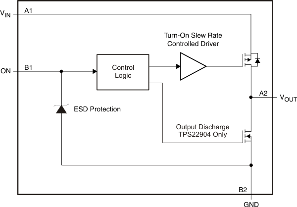
The TPS22903 and TPS22904 are single-channel load switches with controlled turnon.
The devices contain a P-channel MOSFET that can operate over an input voltage range of 1.1 V to 3.6 V. The switch is controlled by an on and off input (ON), which is capable of interfacing directly with low-voltage control signals. In TPS22904, a 85-Ω on-chip load resistor is added for output quick discharge when switch is turned off. Both devices are available in a space-saving 4-terminal WCSP 0.4-mm pitch (YFP).
9.2 Functional Block Diagram

9.3 Feature Description
9.3.1 ON/OFF Control
The ON pin controls the state of the switch. Activating ON continuously holds the switch in the ON-state as there is no fault. ON is active-high and has a low threshold, making it capable of interfacing with low voltage signals. The ON pin is compatible with standard GPIO logic thresholds. It can be used with any microcontroller with 1.2-V, 1.8-V, 2.5-V, or 3.3-V GPIOs.
9.4 Device Functional Modes
Table 1 lists the VOUT pin connections as determined by the ON pin.
Table 1. Functional Table
| ON (CONTROL INPUT) |
VIN TO VOUT | VOUT TO GND (TPS22904 ONLY) | ||
|---|---|---|---|---|
| L | OFF | ON | ||
| H | ON | OFF | ||