SLVSB49F November 2011 – January 2015 TPS22910A , TPS22912C
PRODUCTION DATA.
- 1 Features
- 2 Applications
- 3 Description
- 4 Simplified Schematic
- 5 Revision History
- 6 Device Comparison Table
- 7 Pin Configuration and Functions
-
8 Specifications
- 8.1 Absolute Maximum Ratings
- 8.2 ESD Ratings
- 8.3 Recommended Operating Conditions
- 8.4 Thermal Information
- 8.5 Electrical Characteristics
- 8.6 Switching Characteristics, Typical
- 8.7 Typical DC Characteristics
- 8.8 Typical AC Characteristics, TPS22910A
- 8.9 Typical AC Characteristics, TPS22912C
- 8.10 Typical AC Characteristics, TPS22913B
- 8.11 Typical AC Characteristics, TPS22913C
- 9 Parameter Measurement Information
- 10Detailed Description
- 11Application and Implementation
- 12Power Supply Recommendations
- 13Layout
- 14Device and Documentation Support
- 15Mechanical, Packaging, and Orderable Information
Package Options
Mechanical Data (Package|Pins)
- YZV|4
Thermal pad, mechanical data (Package|Pins)
Orderable Information
13 Layout
13.1 Layout Guidelines
For best performance, all traces should be as short as possible. To be most effective, the input and output capacitors should be placed close to the device to minimize the effects that parasitic trace inductances may have on normal operation. Using wide traces for VIN, VOUT, and GND helps minimize the parasitic electrical effects along with minimizing the case to ambient thermal impedance.
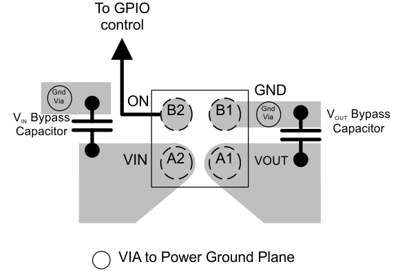
13.2 Layout Example
The figure below shows an example for these devices. Notice the connection to system ground between the VOUT Bypass Capacitor ground and the GND pin of the load switch, this creates a ground barrier which helps to reduce the ground noise seen by the device.
13.3 Thermal Considerations
The maximum IC junction temperature should be restricted to 125°C under normal operating conditions. To calculate the maximum allowable dissipation, PD(max) for a given output current and ambient temperature, use the following equation as a guideline:
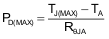
where
- PD(max) = maximum allowable power dissipation
- TJ(max) = maximum allowable junction temperature
- TA = ambient temperature of the device
- θJA = junction to air thermal impedance. See the Thermal Information section. This parameter is highly dependent upon board layout.