SLVSFG2A January   2020  – June 2020 TPS22919-Q1

PRODUCTION DATA.  

  1. Features
  2. Applications
  3. Description
    1.     Device Images
      1.      Simplified Application
  4. Revision History
  5. Pin Configuration and Functions
    1.     Pin Functions
  6. Specifications
    1. 6.1 Absolute Maximum Ratings
    2. 6.2 ESD Ratings
    3. 6.3 Recommended Operating Conditions
    4. 6.4 Thermal Information
    5. 6.5 Electrical Characteristics
    6. 6.6 Switching Characteristics
    7. 6.7 Typical Characteristics
  7. Parameter Measurement Information
    1. 7.1 Test Circuit and Timing Waveforms Diagrams
  8. Detailed Description
    1. 8.1 Overview
    2. 8.2 Functional Block Diagram
    3. 8.3 Feature Description
      1. 8.3.1 On and Off Control
      2. 8.3.2 Output Short Circuit Protection (ISC)
      3. 8.3.3 Fall Time (tFALL) and Quick Output Discharge (QOD)
        1. 8.3.3.1 QOD When System Power is Removed
    4. 8.4 Device Functional Modes
  9. Application and Implementation
    1. 9.1 Application Information
    2. 9.2 Typical Application
      1. 9.2.1 Design Requirements
      2. 9.2.2 Detailed Design Procedure
        1. 9.2.2.1 Limiting Inrush Current
        2. 9.2.2.2 Setting Fall Time for Shutdown Power Sequencing
        3. 9.2.2.3 Application Curves
  10. 10Power Supply Recommendations
  11. 11Layout
    1. 11.1 Layout Guidelines
    2. 11.2 Layout Example
    3. 11.3 Thermal Considerations
  12. 12Device and Documentation Support
    1. 12.1 Trademarks
    2. 12.2 Electrostatic Discharge Caution
    3. 12.3 Glossary
  13. 13Mechanical, Packaging, and Orderable Information

Package Options

Mechanical Data (Package|Pins)
Thermal pad, mechanical data (Package|Pins)
Orderable Information

Typical Characteristics

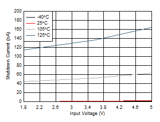
TPS22919-Q1 D001_SLVSEN5.gif
VON ≤ VIL
Figure 1. Shutdown Current vs Input Voltage
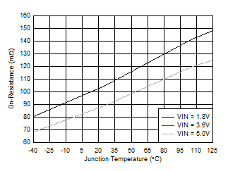
TPS22919-Q1 D003_SLVSEN5.gif
ILOAD = –200 mA
Figure 3. On-Resistance vs Junction Temperature
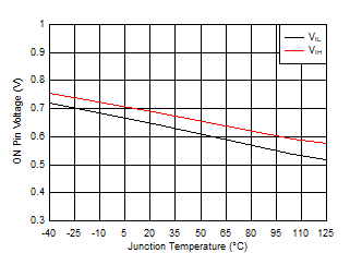
TPS22919-Q1 D005_SLVSEN5.gif
VON ≤ VIL
Figure 5. VIH/VIL vs Junction Temperature
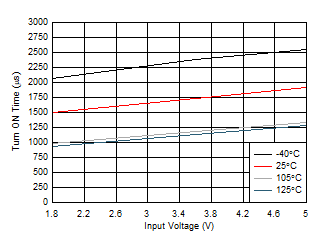
TPS22919-Q1 D007_SLVSEN5.gif
CL = 0.1 μF RL = 100 Ω
Figure 7. Turn ON Time vs Input Voltage
TPS22919-Q1 D009_SLVSEN5.gif
CL = 0.1 μF RL = 100 Ω
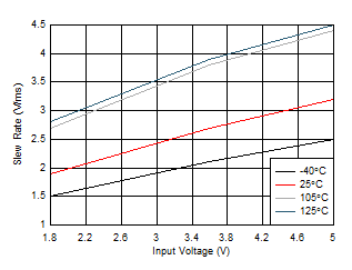
Figure 9. Output Slew Rate vs Input Voltage
TPS22919-Q1 D011_SLVSEN5.gif
RL = 100 Ω TJ = 25°C
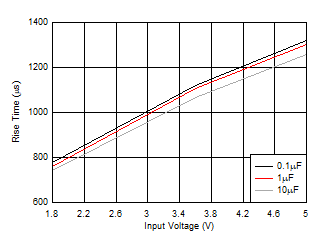
Figure 11. Rise Time vs Input Voltage Across Load Capacitance
TPS22919-Q1 D013_SLVSEN5.gif
CL = 0.1 μF TJ = 25°C
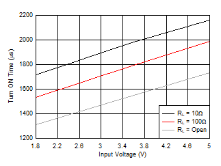
Figure 13. Turn ON Time vs Input Voltage Across Load Resistance
TPS22919-Q1 D015_SLVSEN5.gif
CL = 0.1 μF TJ = 25°C
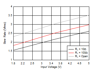
Figure 15. Output Slew Rate vs Input Voltage Across Load Resistance
TPS22919-Q1 D018_SLVSEN5.gif
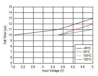
CL = 0.1 μF RL = 100 Ω RPD,QOD = Short
Figure 17. Fall Time vs Input Voltage
TPS22919-Q1 D002_SLVSEN5.gif
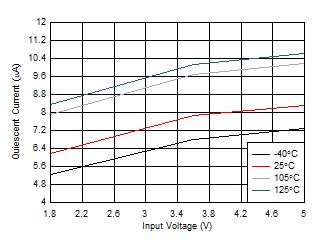
VON ≥ VIH
Figure 2. Quiescent Current vs Input Voltage
TPS22919-Q1 D004_SLVSEN5.gif
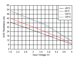
VON ≤ VIL
Figure 4. QOD Resistance vs Input Voltage
TPS22919-Q1 D006_SLVSEN5.gif
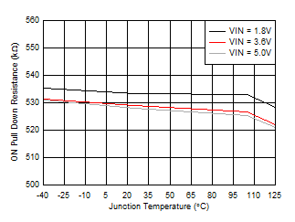
VON ≤ VIL
Figure 6. ON Pull Down Resistance vs Junction Temperature
TPS22919-Q1 D008_SLVSEN5.gif
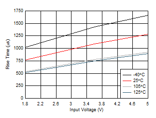
CL = 0.1 μF RL = 100 Ω
Figure 8. Rise Time vs Input Voltage
TPS22919-Q1 D010_SLVSEN5.gif
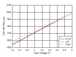
RL = 100 Ω TJ = 25°C
Figure 10. Turn ON Time vs Input Voltage Across Load Capacitance
TPS22919-Q1 D012_SLVSEN5.gif
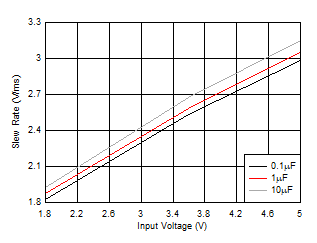
RL = 100 Ω TJ = 25°C
Figure 12. Slew Rate vs Input Voltage Across Load Capacitance
TPS22919-Q1 D014_SLVSEN5.gif
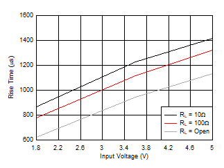
CL = 0.1 μF TJ = 25°C
Figure 14. Rise Time vs Input Voltage Across Load Resistance
TPS22919-Q1 D016_SLVSEN5.gif
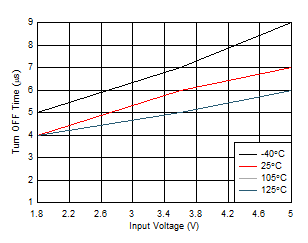
CL = 0.1 μF RL = 100 Ω
Figure 16. Turn OFF Time vs Input Voltage
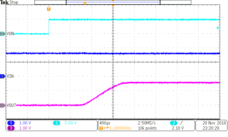
TPS22919-Q1 Rise_1_8.png
CL = 0.1 μF RL = 100 Ω
Figure 18. Rise Time with VIN = 1.8 V
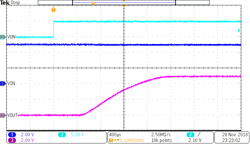
TPS22919-Q1 Rise_5.png
CL = 0.1 μF RL = 100 Ω
Figure 20. Rise Time with VIN = 5 V
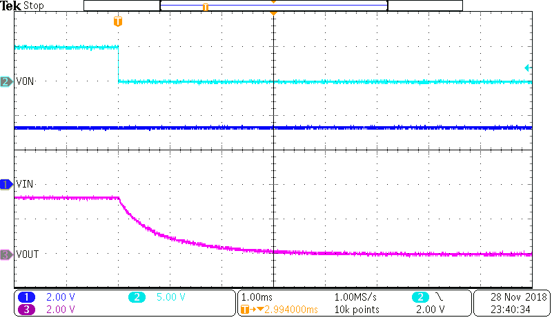
TPS22919-Q1 Fall_Slow.png
CL = 10 μF RL = 100 Ω
Figure 22. Turn Off with a Large Load Capacitance
TPS22919-Q1 Hot_Short.png
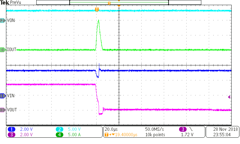
VIN = 3.3 V
Figure 24. Hot Short Event when ON
TPS22919-Q1 Rise_3_3.png
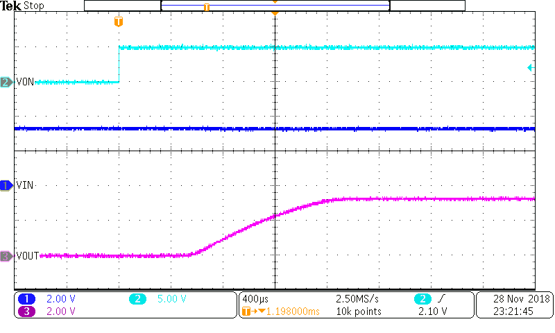
CL = 0.1 μF RL = 100 Ω
Figure 19. Rise Time with VIN = 3.3 V
TPS22919-Q1 Fall_fast.png
CL = Open RL = 100 Ω
Figure 21. Turn Off with a Small Load Capacitance
TPS22919-Q1 Turn_on_short.png
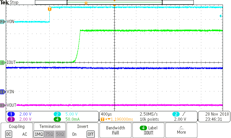
VIN = 3.3 V
Figure 23. Turn On Into an Output Short
TPS22919-Q1 Short_then_Recover.png
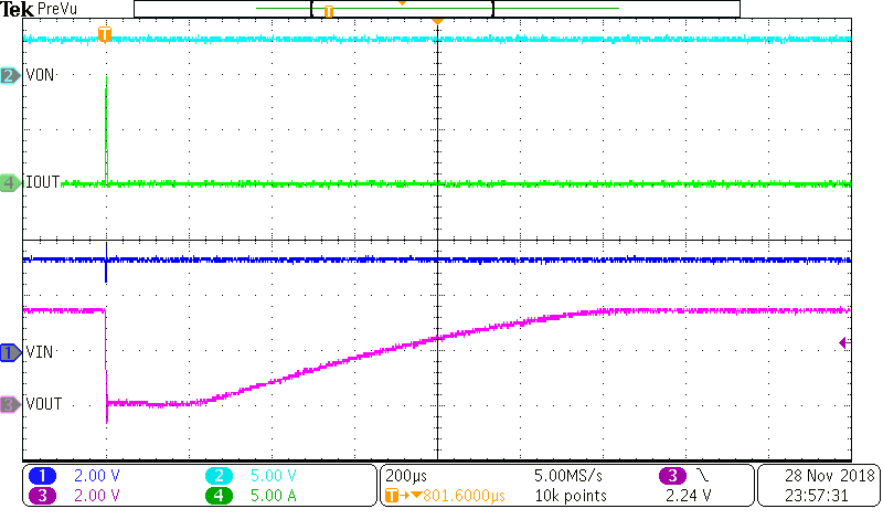
VIN = 3.3 V
Figure 25. Hot Short Event when ON and Recovery