SLVSCT5D March 2015 – September 2016 TPS22953 , TPS22954
PRODUCTION DATA.
- 1 Features
- 2 Applications
- 3 Description
- 4 Revision History
- 5 Device Comparison Table
- 6 Pin Configuration and Functions
-
7 Specifications
- 7.1 Absolute Maximum Ratings
- 7.2 ESD Ratings
- 7.3 Recommended Operating Conditions
- 7.4 Thermal Information
- 7.5 Electrical Characteristics
- 7.6 Electrical Characteristics—VBIAS = 5 V
- 7.7 Electrical Characteristics—VBIAS = 3.3 V
- 7.8 Electrical Characteristics—VBIAS = 2.5 V
- 7.9 Switching Characteristics—CT = 1000 pF
- 7.10 Switching Characteristics—CT = 0 pF
- 7.11 Typical DC Characteristics
- 7.12 Typical Switching Characteristics
- 8 Parameter Measurement Information
-
9 Detailed Description
- 9.1 Overview
- 9.2 Functional Block Diagram
- 9.3
Feature Description
- 9.3.1 On and Off Control (EN pin)
- 9.3.2 Voltage Monitoring (SNS Pin)
- 9.3.3 Power Good (PG Pin)
- 9.3.4 Supervisor Fault Detection and Automatic Restart
- 9.3.5 Manual Restart
- 9.3.6 Thermal Shutdown
- 9.3.7 Reverse Current Blocking (TPS22953 Only)
- 9.3.8 Quick Output Discharge (QOD) (TPS22954 Only)
- 9.3.9 VIN and VBIAS Voltage Range
- 9.3.10 Adjustable Rise Time (CT pin)
- 9.3.11 Power Sequencing
- 9.4 Device Functional Modes
- 10Application and Implementation
- 11Power Supply Recommendations
- 12Layout
- 13Device and Documentation Support
- 14Mechanical, Packaging, and Orderable Information
Package Options
Mechanical Data (Package|Pins)
Thermal pad, mechanical data (Package|Pins)
- DQC|10
Orderable Information
10 Application and Implementation
NOTE
Information in the following applications sections is not part of the TI component specification, and TI does not warrant its accuracy or completeness. TI’s customers are responsible for determining suitability of components for their purposes. Customers should validate and test their design implementation to confirm system functionality.
10.1 Application Information
This section will highlights some of the design considerations when implementing this device in various applications. A PSPICE model for this device is also available on www.ti.com for further aid.
10.1.1 Input to Output Voltage Drop
The input to output voltage drop in the device is determined by the RON of the device and the load current. The RON of the device depends upon the VIN and VBIAS conditions of the device. Refer to the RON specification of the device in the Electrical Characteristics table of this datasheet. Once the RON of the device is determined based upon the VIN and VBIAS voltage conditions, use Equation 5 to calculate the input to output voltage drop.

where
- ΔV is the voltage drop from IN to OUT
- ILOAD is the load current
- RON is the On-Resistance of the device for a specific VIN and VBIAS
An appropriate ILOAD must be chosen such that the IMAX specification of the device is not violated.
10.1.2 Thermal Considerations
The maximum IC junction temperature must be restricted to just under the thermal shutdown (TSD) limit of the device. To calculate the maximum allowable dissipation, PD(max) for a given output current and ambient temperature, use Equation 6.

where
- PD(max) is the maximum allowable power dissipation
- TJ(max) is the maximum allowable junction temperature before hitting thermal shutdown (see the Electrical Characteristics table)
- TA is the ambient temperature of the device
- θJA is the junction to air thermal impedance. See the Thermal Information section. This parameter is highly dependent upon board layout.
10.1.3 Automatic Power Sequencing
The PG pin of the TPS22953/54 allows for automatic sequencing of multiple system rails or loads. The accurate SNS voltage monitoring ensures the first rail is up before the next starts to turn on. This approach provides robust system sequencing and reduces the total inrush current by preventing overlap. Figure 60 shows how two rails can be sequenced. There is no limit to the number of rails that can be sequenced in this way
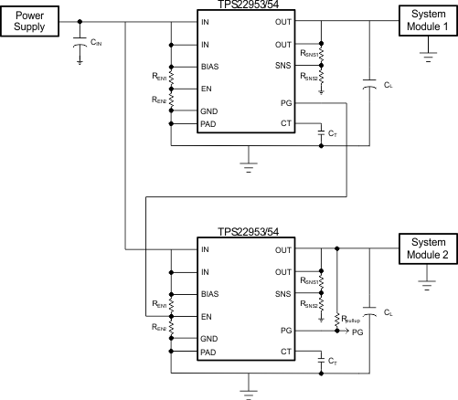 Figure 60. Power Sequencing with PG Control Schematic
10.1.4 Monitoring a Downstream Voltage
The SNS pin can be used to monitor other system voltages in addition to VOUT. The status of the monitored voltage are indicated by the PG pin which can be pulled up to VOUT or another voltage. Figure 61 shows an example of the TPS22953/54 monitoring the output of a downstream DC/DC regulator. In this case, the switch turns on when the power supply is above the UVLO, but the PG is not asserted until the DC/DC regulator has started up.
 Figure 61. Monitoring a Downstream Voltage Schematic
In this application, if the DC/DC Regulator is shut down, the supervisor registers this as a fault case and reset the load switch.
10.1.5 Monitoring the Input Voltage
The SNS pin can also be used to monitor VIN in the case a MCU GPIO is being used to control the EN. This allows PG to report on the status of the input voltage when the switch is enabled. See Figure 62.
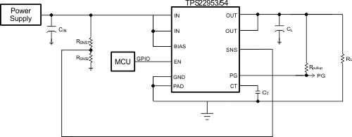 Figure 62. Monitoring The Input Voltage Schematic
10.1.6 Break-Before-Make Power MUX (TPS22953 Only)
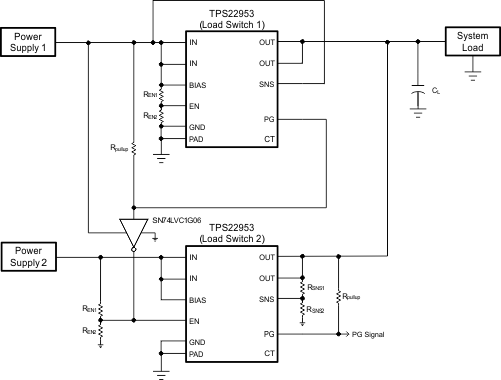
The reverse current blocking feature of the TPS22953 makes it suitable for power multiplexing (MUXing) between two power supplies with different voltages. The SNS and PG pin can be configured to implement break-before-make logic. The circuit in Figure 63 shows how the detection of Power Supply 1 can be used to disable the load switch for Power Supply 2. By tying the SNS of Load Switch 1 directly to the input, its PG pin is pulled up as soon as the device is enabled.
The break-before-make logic ensures that Power Supply 2 is completely disconnected before Power Supply 1 is connected. This approach provides very robust reverse current blocking. However, in most cases, this also results in a dip in the output voltage when switching between supplies.
The amount of voltage dip depends on the loading, the output capacitance, and the turnon delay of the load switch. In this application, leaving the CT pin open results in the shortest turn on delay and minimize the output voltage dip.
Table 3 summarizes the logic of the PG Signal for Figure 63.
Table 3. Break-Before-Make PG Signal
| PG Signal | Indication |
|---|---|
| H | Power supply 1 not present. System powered from power supply 2. |
| L | Power supply 1 present. System powered from power supply 1. |
10.1.7 Make-Before-Break Power MUX (TPS22953 Only)
The reverse current blocking feature of the TPS22953 makes it suitable for power multiplexing (MUXing) between two power supplies with different voltages. The SNS and PG pin can be configured to implement make-before-break logic. The circuit in Figure 64 shows how the detection of Load Switch 1 turning on can be used to disable the load switch for Power Supply 2. By tying SNS to the Load, the PG is pulled up when the output voltage starts to rise. This disables an active low load switch such as the TPS22910A.
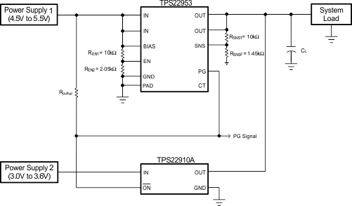 Figure 64. Make-Before-Break Power MUX Schematic
The make-before-break logic ensures that Power Supply 2 is not disconnected until Power Supply 1 is connected. Unlike break-before-make logic, this approach is ideal for preventing voltage dip on the output when switching between supplies. However, in most cases, this also results in temporary reverse current flow.
The TPS22910A is well suited for this application because it can detect and block reverse current even before it is disabled by the TPS22953 PG signal. Also, the active low enable of the TPS22910A eliminates the need for an inverter as shown in the previous example.
In order to ensure correct logic, the SNS pin must be configured to toggle PG when the load voltage is between the two supply voltages (3.6 V to 4.5 V). The SNS resistor values in Figure 64 are assuming a tolerance of ±1% or better.
Table 4 summarizes the logic of the PG Signal for Figure 64.
Table 4. Make-Before-Break PG Signal
| PG Signal | Indication |
|---|---|
| H | Power supply 1 present. System powered from power supply 1. |
| L | Power supply 1 not present. System powered from power supply 2. |
10.2 Typical Application
This application demonstrates how the TPS22953/54 can use used to limit inrush current to output capacitance.
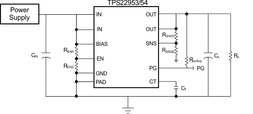 Figure 65. Powering a Downstream Module Schematic
10.2.1 Design Requirements
For this design example, use the input parameters shown in Table 5.
Table 5. Design Parameters
| DESIGN PARAMETER | EXAMPLE VALUE |
|---|---|
| VIN | 3.3 V |
| VBIAS | 5 V |
| CL | 47 µF |
| Maximum Acceptable Inrush Current | 150 mA |
| RL | None |
10.2.2 Detailed Design Procedure
To begin the design process, the designer needs to know the following:
- Input voltage
- BIAS voltage
- Load current
- Load capacitance
- Maximum acceptable inrush current
10.2.2.1 Inrush Current
To determine how much inrush current is caused by the CL capacitor, use Equation 7.

where
- IINRUSH is the amount of inrush caused by CL
- CL is the load capacitance on VOUT
- dt is the VOUT Rise Time (typically 10% to 90%)
- dVOUT is the Change in VOUT Voltage (typically 10% to 90%)
In this case, a Slew Rate slower than 314 μs/V is required to meet the maximum acceptable inrush requirement. Equation 4 can be used to estimate the CT capacitance (as shown in Equation 8 and Equation 9) required for this slew rate.
10.2.3 Application Curves
The following Application Curves show the inrush with multiple different CT values. These curves show only a CT capacitance greater than 840 pF results in the acceptable inrush current of 150 mA.
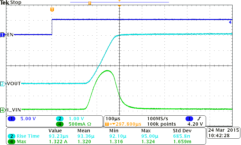
| CT = 0 pF | ||
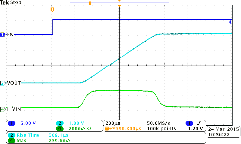
| CT = 470 pF | ||
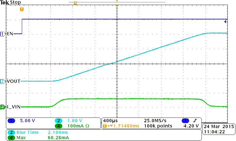
| CT = 2200 pF | ||
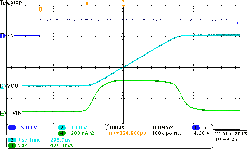
| CT = 220 pF | ||
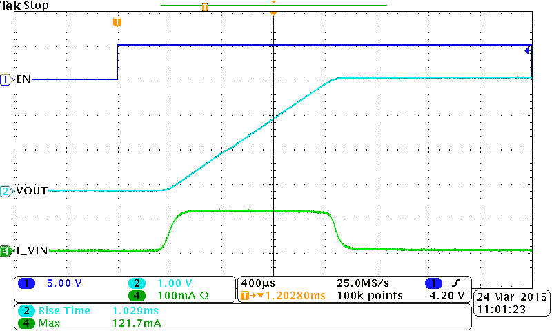
| CT = 1000 pF | ||
