SLVSCI4B February 2014 – September 2014 TPS22961
PRODUCTION DATA.
- 1 Features
- 2 Applications
- 3 Description
- 4 Simplified Schematic
- 5 Revision History
- 6 Terminal Configuration and Functions
- 7 Specifications
- 8 Detailed Description
- 9 Applications and Implementation
- 10Power Supply Recommendations
- 11Layout
- 12Device and Documentation Support
- 13Mechanical, Packaging, and Orderable Information
Package Options
Refer to the PDF data sheet for device specific package drawings
Mechanical Data (Package|Pins)
- DNY|8
Thermal pad, mechanical data (Package|Pins)
Orderable Information
11 Layout
11.1 Layout Guidelines
- VIN and VOUT traces should be as short and wide as possible to accommodate for high current.
- Use vias under the exposed thermal pad for thermal relief for high current operation.
- The VIN terminal should be bypassed to ground with low ESR ceramic bypass capacitors. The typical recommended bypass capacitance is 1-µF ceramic with X5R or X7R dielectric. This capacitor should be placed as close to the device terminals as possible.
- The VOUT terminal should be bypassed to ground with low ESR ceramic bypass capacitors. The typical recommended bypass capacitance is one-tenth of the VIN bypass capacitor of X5R or X7R dielectric rating. This capacitor should be placed as close to the device terminals as possible.
- The VBIAS terminal should be bypassed to ground with low ESR ceramic bypass capacitors. The typical recommended bypass capacitance is 0.1-µF ceramic with X5R or X7R dielectric.
11.2 Layout Example
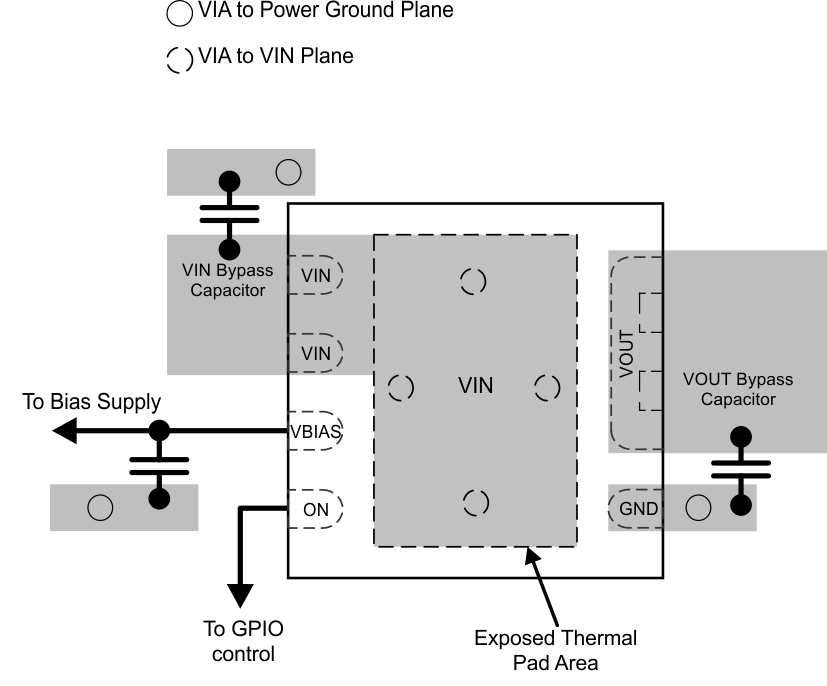 Figure 33. Recommended Board Layout